


AD9912
Rev. D | Page 34 of 40
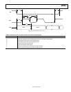
CMOS OUTPUT DIVIDER (S-DIVIDER) (REGISTER 0x0100 TO REGISTER 0x0106)
Register 0x0100 to Register 0x0103—Reserved
Register 0x0104—S-Divider
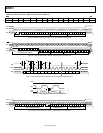
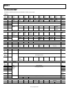
Table 21.
Bits Bit Name Description
[7:0] S-divider CMOS output divider. Divide ratio = 1 − 65,536. If the desired S-divider setting is greater than 65,536,
or if the signal on FDBK_IN is greater than 400 MHz, then Bit 0 in Register 0x0106 must be set. Note that
the actual S-divider is the value in this register plus 1; so to have an S-divider of 1, Register 0x0104 and
Register 0x0105 must both be 0x00. Register 0x0104 is the least significant byte.
Register 0x0105—S-Divider (Continued)
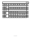
Table 22.
Bits Bit Name Description
[15:8] S-divider CMOS output divider. Divide ratio = 1 − 65,536. If the desired S-divider setting is greater than 65,536,
or if the signal on FDBK_IN is greater than 400 MHz, then Bit 0 in Register 0x0106 must be set. Note that
the actual S-divider is the value in this register plus 1; so to have an S-divider of 1, Register 0x0104 and
Register 0x0105 must both be 0x00. Register 0x104 is the least significant byte.
Register 0x0106—S-Divider (Continued)
Table 23.
Bits Bit Name Description
7 Falling edge triggered Setting this bit inverts the reference clock before S-divider.
[6:1] Reserved Reserved.
0 S-divider/2 Setting this bit enables an additional /2 prescaler. See the CMOS Output Divider (S-Divider) section.
If the desired S-divider setting is greater than 65,536, or if the signal on FDBK_IN is greater than 400 MHz,
this bit must be set.
FREQUENCY TUNING WORD (REGISTER 0x01A0 TO REGISTER 0x01AD)
Register 0x01A0 to Register 0x01A5—Reserved
Register 0x01A6—FTW0 (Frequency Tuning Word)
Table 24.
Bits Bit Name Description
[7:0] FTW0 These registers contain the FTW (frequency tuning word) for the DDS. The FTW determines the ratio
of the AD9912 output frequency to its DAC system clock. Register 0x01A6 is the least significant byte
of the FTW. Note that the power-up default is defined by start-up Pin S1 to Pin S4. Updates to the FTW
results in an instantaneous frequency jump but no phase discontinuity.
Register 0x01A7—FTW0 (Frequency Tuning Word) (Continued)
Table 25.
Bits Bit Name Description
[15:8] FTW0 These registers contain the FTW (frequency tuning word) for the DDS. The FTW determines the ratio
of the AD9912 output frequency to its DAC system clock. Register 0x01A6 is the least significant byte
of the FTW. Note that the power-up default is defined by start-up Pin S1 to Pin S4. Updates to the FTW
results in an instantaneous frequency jump but no phase discontinuity.
Register 0x01A8—FTW0 (Frequency Tuning Word) (Continued)
Table 26.
Bits Bit Name Description
[23:16] FTW0 These registers contain the FTW (frequency tuning word) for the DDS. The FTW determines the ratio
of the AD9912 output frequency to its DAC system clock. Register 0x01A6 is the least significant byte
of the FTW. Note that the power-up default is defined by start-up Pin S1 to Pin S4. Updates to the FTW
results in an instantaneous frequency jump but no phase discontinuity.