


AD9912
Rev. D | Page 29 of 40
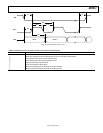
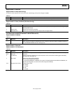
06763-048
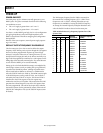
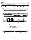
CSB
SCLK
SDIO
t
HIGH
t
LOW
t
CLK
t
S
t
DS
t
DH
t
H
BIT N BIT N + 1
Figure 56. Serial Control Port Timing—Write
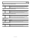
Table 11. Definitions of Terms Used in Serial Control Port Timing Diagrams
Parameter Description
t
CLK
Period of SCLK
t
DV
Read data valid time (time from falling edge of SCLK to valid data on SDIO/SDO)
t
DS
Setup time between data and rising edge of SCLK
t
DH
Hold time between data and rising edge of SCLK
t
S
Setup time between CSB and SCLK
t
H
Hold time between CSB and SCLK
t
HI
Minimum period that SCLK should be in a logic high state
t
LO
Minimum period that SCLK should be in a logic low state