


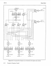
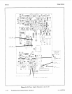
Model
8904A
Service
R202 t15V
4
0201
R204
+15V
0202
I
c207
R205
TI
R206
c208
II
I
-
b
-
dl
61
c221 CR206 CR203
0205
+bV
0206
FROM
CLOCK
SYNC U2A
(HIGH TRUE)
HI
-
R226
-15V
4)
-
tI
-
II
-
-
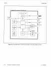
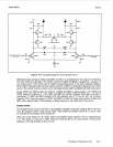
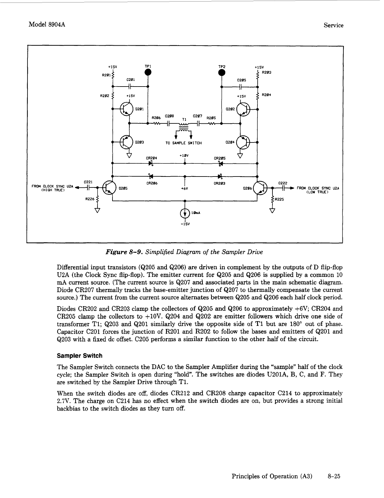
Figure
8-9.
Simplified Diagram
of
the Sampler Drive
Differential input transistors
(Q205
and
Q206)
are driven in complement by the outputs of
D
flip-flop
U2A
(the Clock Sync flip-flop). The emitter current
for
Q205
and
Q206
is
supplied by a common
10
mA current source. (The current source is
Q207
and
associated parts in the main schematic diagram.
Diode
CR207
thermally tracks the base-emitter junction of
Q207
to
thermally compensate the current
source.) The current from the current source alternates between
Q205
and
Q206
each half clock period.
Diodes
CR202
and
CR203
clamp the collectors of
Q205
and
Q206
to approximately
+6V; CR204
and
CR205
clamp the collectors to
+lOV.
Q204
and
Q202
are emitter followers which drive one side
of
transformer
T1;
Q203
and
Q201
similarly drive
the
opposite side of
T1
but are
180”
out of phase.
Capacitor
C201
forces the junction of
R201
and
R202
to follow the bases and emitters of
Q201
and
Q203
with a fixed dc offset.
C205
performs a similar function to the other half of the circuit.
Sampler
Switch
The Sampler Switch connects the
DAC
to
the Sampler Amplifier during the “sample” half of the clock
cycle; the Sampler Switch
is
open during “hold”. The switches are diodes
U201A,
B,
C,
and
F.
They
are switched by the Sampler Drive through
T1.
When the switch diodes are
off,
diodes
CR212
and
CR208
charge capacitor
C214
to approximately
2.7V.
The charge on
C214
has no effect when the switch diodes are on, but provides a strong initial
backbias to the switch diodes as they turn
off.
Principles
of
Operation
(A3)
8-25