


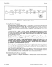
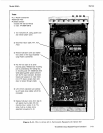

Service Model 8904A
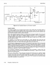
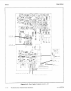
Floating Amplifier Driver and On/Off Switch (Service Sheet
3)
The On/Off Switch is opened for 15 ms when the Sharp Cutoff Filter is in and the frequency of the
signal is changed to prevent the ringing in the filter from getting to the instrument’s output.
The unity-gain, inverting buffer amplifier formed by U403 and U404 isolates the Floating Output
Amplifier from the Sine
X/X
Compensation. The combination of resistors R412, R413, and R421 form
a
1
kR resistance which can handle the output current from the Audio Amplifier. U404 is a current
booster stage. C401 bypasses U404 at high frequencies to stabilize the buffer
at
high frequencies. L401
and R416 compensate the high-frequency rolloff of the Floating Output Amplifier.
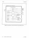
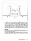
Floating Output Amplifier (Service Sheet
4)
The Floating Output Amplifier is a single-ended-to-differential converter. Conversion
is
accomplished
by a precise combination of negative feedback, positive feedback, and cross-coupling which yields a
symmetrical differential output with high common-mode rejection and a well-defined output impedance
of 50R. The complexity of the circuit makes detailed analysis difficult.
Output transistors Q401 through Q404 boost the current drive capability of differential amplifiers U401
and U402. Constant-current sources CR423 through CR426 provide bias current
for
diodes CR404
through CR407 and the bases of Q401 through Q404. CR423 through CR426 thermally compensate the
base-emitter junctions of Q401 through Q404. Q405 through Q408 shut
off
Q401 through Q404 when
the latter transistors start drawing too much current to protect the amplifier. Further protection
is
provided by CR408 through CR411 and CR419 through CR422. C425 equalizes the phase shift through
the upper and lower portions of the amplifier for best high-frequency balance.
The +16 and -16V power supply regulators (Q300 and Q301) supply current to only the amplifier. This
minimizes the effects of the large-current needs of the amplifier on the other circuits and minimizes
distortion.
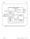
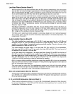
Overvoltage Protection and Output Circuits (Service Sheet
4)
Between the Floating Output Amplifier and the output connectors are several circuits.
Balun T400 improves the balance of the Floating Output Amplifier at high frequencies where the
amplifier’s balance has deteriorated.
The 48
dB
Attenuator
is
a 500, pi-section attenuator. C505 compensates the high-frequency effects of
the parasitic capacitance of the contacts of K8.
The Overvoltage Protection Circuits open the relays on the
two
output lines when a large voltage
is
inadvertently applied to an output connector. The circuit thus protects the instrument’s output circuits
(especially the Floating Output Amplifier). Application of a large voltage on the output
is
sensed (after
attenuation by voltage dividers R490 and R491 and R492 and R493) by comparators U400A through
U400D which are referenced to voltages from the voltage dividers R495 and R497 and R494 and R496.
Both positive and negative references are sensed on both output lines. When a comparator trips, K402A
and K402B are opened via flip-flop U2B and drivers UlOG, U8D and U8E. U2B also turns on Q33
which
is
read
by
the controller to generate an error message on the instrument’s display. CR415 through
CR418 protect the comparators. VR31 shifts the comparators’ outputs to a TTL level. C440 and C441
prevent arcing of the contacts of K402 when the relay is deactivating. C64, CR17, CR18, and R122
open K402 at instrument turn-on.
Components C409 through C413 and L402 prevent high-frequency parasitic signals on the high-output
line from radiating from the instrument.
Relay K404A controls the float
or
ground state of the low-output line.
8-28
Principles
of
Operation
(A3)