


16-BIT TIMER 1(0,1) S3C84E5/C84E9/P84E9
12-2
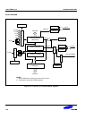
FUNCTION DESCRIPTION
Timer 1(0,1) Interrupts (IRQ2, Vectors C4H, C6H, C8H and CAH)
The timer 1(0) module can generate two interrupts, the timer 1(0) overflow interrupt (T1OVF0), and the timer 1(0)
match/capture interrupt (T1INT0). T1OVF0 is interrupt level IRQ2, vector C6H. T1INT0 also belongs to interrupt level
IRQ2, but is assigned the separate vector address, C4H.
A timer 1(0) overflow interrupt pending condition is automatically cleared by hardware when it has been serviced. A
timer 1(0) match/capture interrupt, T1INT0 pending condition is also cleared by hardware when it has been serviced.
The timer 1(1) module can generate two interrupts, the timer 1(1) overflow interrupt (T1OVF1), and the timer 1(1)
match/capture interrupt (T1INT1). T1OVF1 is interrupt level IRQ2, vector CAH. T1INT1 also belongs to interrupt level
IRQ2, but is assigned the separate vector address, C8H.
A timer 1(1) overflow interrupt pending condition is automatically cleared by hardware when it has been serviced. A
timer 1(1) match/capture interrupt, T1INT1 pending condition is also cleared by hardware when it has been serviced.
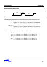
Interval Mode (match)
The timer 1(0) module can generate an interrupt: the timer 1(0) match interrupt (T1INT0). T1INT0 belongs to interrupt
level IRQ2, and is assigned the separate vector address, C4H. In interval timer mode, a match signal is generated
and T1OUT0 is toggled when the counter value is identical to the value written to the Timer 1 reference data
registers, T1DATAH0 and T1DATAL0. The match signal generates a timer 1(0) match interrupt (T1INT0, vector C4H)
and clears the counter value.
The timer 1(1) module can generate an interrupt: the timer 1(1) match interrupt (T1INT1). T1INT1 belongs to interrupt
level IRQ2, and is assigned the separate vector address, C8H. In interval timer mode, a match signal is generated
and T1OUT1 is toggled when the counter value is identical to the value written to the Timer 1 reference data register,
T1DATAH1 and T1DATAL1. The match signal generates a timer 1(1) match interrupt (T1INT1, vector C8H) and clears
the counter value.
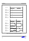
Capture Mode
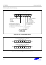
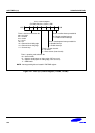
In capture mode for timer 1(0), a signal edge that is detected at the T1CAP0 pin opens a gate and loads the current
counter value into the timer 1 data registers (T1DATAH0, T1DATAL0 for rising edge, or falling edge). You can select
rising or falling edge to trigger this operation. The timer 1(0) also gives you capture input source, the signal edge at
the T1CAP0 pin. You select the capture input by setting the value of the timer 1(0) capture input selection bit in the
port 0 control register high, P0CONH, (set 1 bank0, E6H).
Both kinds of timer 1(0) interrupts (T1OVF0, T1INT0) can be used in capture mode, the timer 1(0) overflow interrupt is
generated whenever a counter overflow occurs, the timer 1(0) capture interrupt is generated whenever the counter
value is loaded into the timer 1 data register.
By reading the captured data value in T1DATAH0, T1DATAL0, and assuming a specific value for the timer 1(0) clock
frequency, you can calculate the pulse width (duration) of the signal that is being input at the T1CAP0 pin.
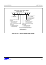
In capture mode for Timer 1(1), a signal edge that is detected at the T1CAP1 pin opens a gate and loads the current
counter value into the timer 1 data register (T1DATAH1, T1DATAL1 for rising edge, or falling edge). You can select
rising or falling edges to trigger this operation. The timer 1(1) also gives you capture input source, the signal edge at
the T1CAP1 pin. You select the capture input by setting the value of the timer 1(1) capture input selection bit in the
port 0 control register low, P0CONL, (set 1 bank0, E7H).
Both kinds of timer 1(1) interrupts (T1OVF1, T1INT1) can be used in capture mode, the timer 1(1) overflow interrupt is
generated whenever a counter overflow occurs, the timer 1(1) capture interrupt is generated whenever the counter
value is loaded into the timer 1 data register.
By reading the captured data value in T1DATAH1, T1DATAL1, and assuming a specific value for the timer 1(1) clock
frequency, you can calculate the pulse width (duration) of the signal that is being input at the T1CAP1 pin.