


S3C84E5/C84E9/P84E9 16-BIT TIMER 1(0,1)
12-3
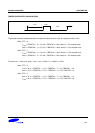
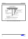
PWM Mode
Pulse width modulation (PWM) mode lets you program the width (duration) of the pulse that is output at the
T1OUT0, T1OUT1 pin. As in interval timer mode, a match signal is generated when the counter value is identical to
the value written to the timer 1(0,1) data registers. In PWM mode, however, the match signal does not clear the
counter but can generate a match interrupt. Instead, it runs continuously, overflowing at FFFFH, and then continuous
increasing from 0000H. Whenever an overflow occur, an overflow (T1OVF0,1) interrupt can be generated.
Although you can use the match or overflow interrupts in the PWM mode, these interrupts are not typically used in
PWM-type applications. Instead, the pulse at the T1OUT0, T1OUT1 pin is held to low level as long as the reference
data value is less than or equal to(≤) the counter value and then the pulse is held to high level for as long as the data
value is greater than(>) the counter value. One pulse width is equal to t
CLK.
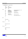
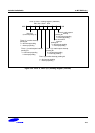
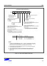
TIMER 1(0,1) CONTROL REGISTER (T1CON0, T1CON1)
You use the timer 1(0,1) control register, T1CON0, T1CON1, to:
— Select the timer 1(0,1) operating mode (Interval timer, Capture mode, PWM mode)
— Select the timer 1(0,1) input clock frequency
— Clear the timer 1(0,1) counter, T1CNTH0/L0, T1CNTH1/L1
— Enable the timer 1(0,1) overflow interrupt
— Enable the timer 1(0,1) match/capture interrupt
T1CON0 is located in set 1 and Bank 1 at address E8H, and is read/write addressable using Register addressing
mode. T1CON1 is located in set 1 and Bank 1 at address E9H, and is read/write addressable using Register
addressing mode.
A reset clears T1CON0, T1CON1 to ‘00H’. This sets timer 1(0,1) to normal interval timer mode, selects an input
clock frequency of fxx/1024, and disables all timer 1(0,1) interrupts. To disable the counter operation, please set
T1CON(0,1).7-.5 to 111B. You can clear the timer 1(0,1) counter at any time during normal operation by writing a “1”
to T1CON(0,1).3.
The timer 1(0) overflow interrupt (T1OVF0) is interrupt level IRQ2 and has the vector address C6H. And, the timer 1(1)
overflow interrupt (T1OVF1) is interrupt level IRQ2 and has the vector address CAH.
To generate the exact time interval, you should write “1” to T1CON(0,1).2 and clear appropriate pending bits of the
TINTPND register.
To detect a match/capture or overflow interrupt pending condition when T1INT0, T1INT1 or T1OVF0, T1OVF1 is
disabled, the application program should poll the pending bit TINTPND register, bank 1, address E0H.
When a “1” is detected, a timer 1(0,1) match/capture or overflow interrupt is pending. When the sub-routine has been
serviced, the pending condition must be cleared by software by writing a “0” to the interrupt pending bit. If interrupts
(match/capture or overflow) are enabled, the pending bit is cleared automatically by hardware.