


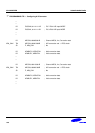

ELECTRICAL DATA S3C84E5/C84E9/P84E9
17-6
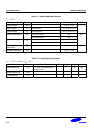
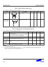
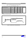
Table 17-5. Main Oscillator Frequency (f
OSC1
)
(T
A
= – 25 °C + 85 °C, V
DD
= V
LVR
to 5.5 V)
Oscillator Clock Circuit Test Condition Min Typ. Max Unit
Main crystal or
ceramic
X
IN
C1 C2
X
OUT
V
DD
= V
LVR
to 5.5 V
1 – 12 MHz
External clock
(main system)
X
IN
X
OUT
V
DD
= V
LVR
to 5.5 V
1 – 12
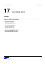
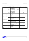
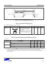
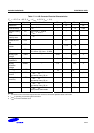
Table 17-6. Main Oscillator Clock Stabilization Time (t
ST1
)
(T
A
= – 25 °C + 85 °C, V
DD
= V
LVR
to 5.5 V)
Oscillator Test Condition Min Typ. Max Unit
Main crystal
f
OSC
> 400 kHz;
Oscillation stabilization occurs when V
DD
is equal
to the minimum oscillator voltage range.
– – 10 ms
Main ceramic – – 4
External clock
(main system)
X
IN
input High and Low width (t
XH
, t
XL
)
50 – – ns
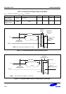
Oscillator
stabilization
wait time
t
WAIT
when released by a reset
(1)
–
2
16
/f
OSC
– sec
t
WAIT
when released by an interrupt
(2)
–
–
– sec
NOTES:
1. f
OSC
is the oscillator frequency.
2. The duration of the oscillator stabilization wait time, t
WAIT
, when it is released by an interrupt is determined by the
settings in the basic timer control register, BTCON.