


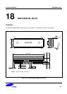
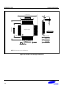
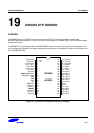
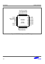

S3C84E5/C84E9/P84E9 OTP VERSION
19-3
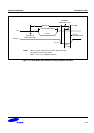
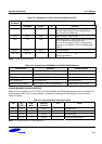
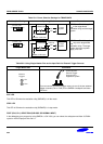
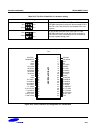
Table 19-1. Descriptions of Pins Used to Read/Write the OTP
Main Chip
Pin Name
During Programming
Pin Name Pin No. I/O Function
P4.3 SDAT 9(3) I/O Serial data pin. Output port when reading and
input port when writing. Can be assigned as a
input or push-pull output port.
P4.2 SCLK 10(4) I Serial clock pin. Input only pin.
TEST
V
PP
15(9) I Power supply pin for EPROM cell writing (indicates
that OTP enters into the writing mode).
When 12.5 V is applied, OTP is in writing mode
and when 5 V is applied, OTP is in reading mode.
(Option)
nRESET nRESET 18(12) I Chip Initialization
V
DD
/V
SS
V
DD
/V
SS
11(12)/5(6) –
Logic power supply pin. V
DD
should be tied to +5 V
during programming.
NOTE: ( ) means 44 QFP package.
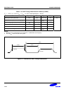
Table 19-2. Comparison of S3P84E9 and S3C84E5/C84E9 Features
Characteristic S3P84E9 S3C84E5/C84E9
Program memory 32K-byte EPROM 16/32K-byte mask ROM
Operating voltage (V
DD
) V
LVR
to 5.5 V V
LVR
to 5.5 V
OTP programming mode
V
DD
= 5 V, V
PP
(TEST) = 12.5 V
Pin configuration 42-SDIP/44-QFP 42-SDIP/44-QFP
EPROM programmability User Program 1 time by programmer Programmed at the factory
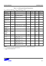
OPERATING MODE CHARACTERISTICS
When 12.5 V is supplied to the V
PP
(TEST) pin of the S3P84E9, the EPROM programming mode is entered. The
operating mode (read, write, or read protection) is selected according to the input signals to the pins listed in
Table 19-3 below.
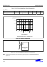
Table 19-3. Operating Mode Selection Criteria
V
DD
V
PP
(TEST)
REG/
MEM
Address
(A14–A0)
R/W Mode
5 V 5 V 0 xxxxH 1 EPROM read
12.5 V 0 xxxxH 0 EPROM program
12.5 V 0 xxxxH 1 EPROM verify
12.5 V 1 0E3FH 0 EPROM read protection
NOTE: "0" means Low level; "1" means High level.