


S3C84E5/C84E9/P84E9 A/D CONVERTER
15-5
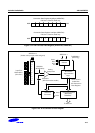
INTERNAL A/D CONVERSION PROCEDURE
1. Analog input must remain between the voltage range of AVSS and AVREF.
2. Configure P3.0–P3.7 for analog input before A/D conversions. To do this, you load the appropriate value to the
P3CONH and P3CONL (for ADC0–ADC7) registers.
3. Before the conversion operation starts, you must first select one of the eight input pins (ADC0–ADC7) by writing
the appropriate value to the ADCON register.
4. When conversion has been completed, (50 clocks have elapsed), the EOC, ADCON.3 flag is set to "1", so that
a check can be made to verify that the conversion was successful.
5. The converted digital value is loaded to the output register, ADDATAH (8-bit) and ADDATAL (2-bit), then the ADC
module enters an idle state.
6. The digital conversion result can now be read from the ADDATAH and ADDATAL register.
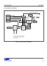
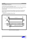
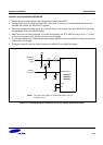
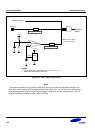
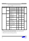
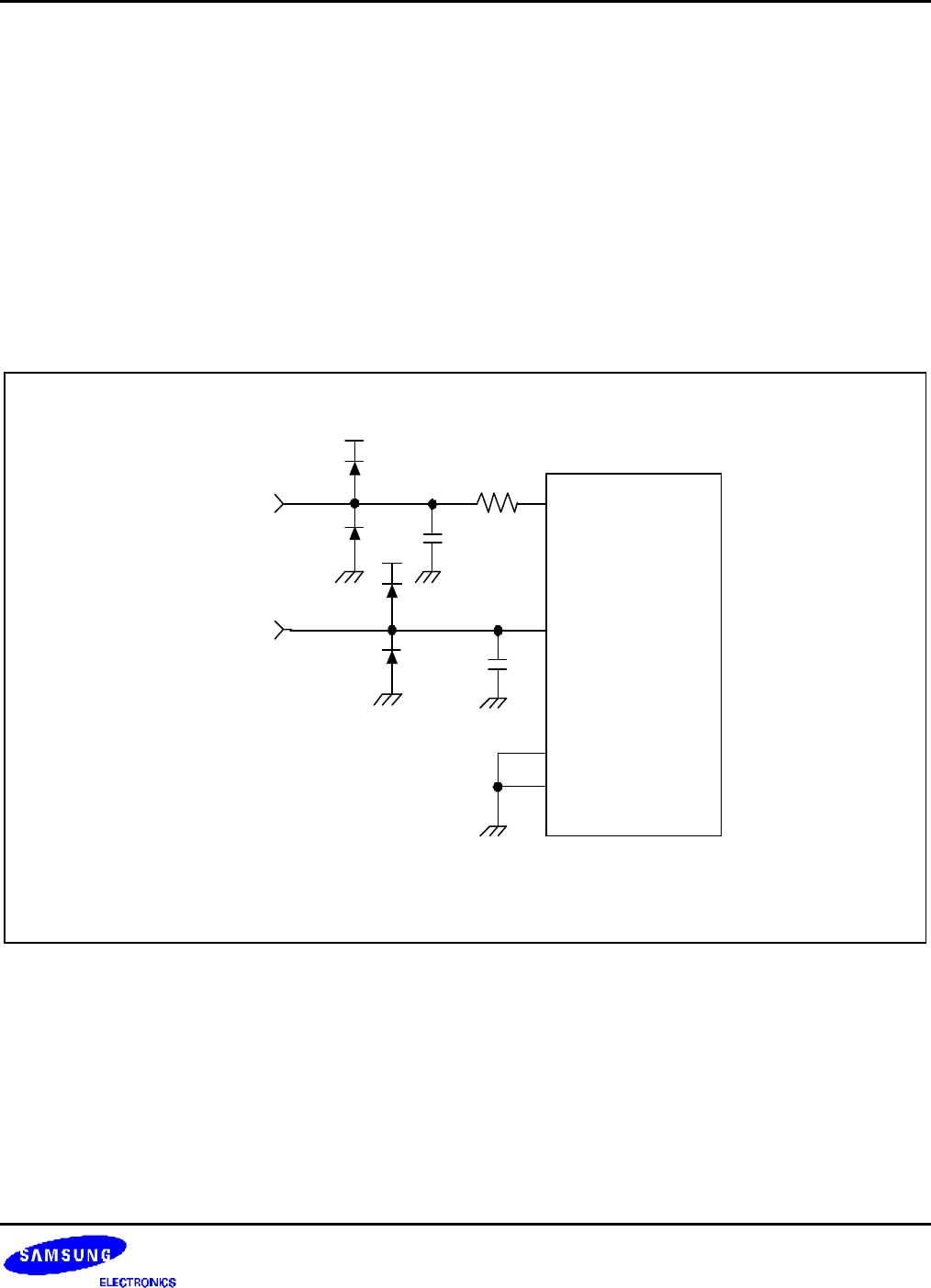
Reference
Voltage
Input
Analog
Input Pin
NOTE:
The symbol "R" signifies an offset resistor with a value of
from 50 to 100
Ω
.
Vss
S3C84E5/
S3C84E9/
S3P84E9
ADC0-ADC7
AVref
R
VDD
VDD
104
101
AVss
Figure 15-5. Recommended A/D Converter Circuit for Highest Absolute Accuracy