


ELECTRICAL DATA S3C84E5/C84E9/P84E9
17-4
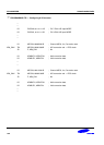
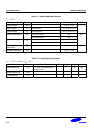
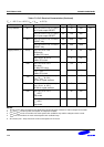
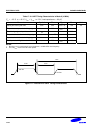
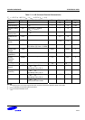
Table 17-3. D.C. Electrical Characteristics (Continued)
(T
A
= – 25 °C to + 85 °C, V
DD
= V
LVR
to 5.5 V)
Parameter Symbol Conditions Min Typ. Max Unit
Pull-up resistor
R
P1
V
DD
= 5 V; V
IN
= 0 V, T
A
= 25°C
All I/O pins except nRESET
10 50 100
kΩ
V
DD
= 3 V; V
IN
= 0 V, T
A
= 25°C
All I/O pins except nRESET
20 100 400
R
P2
V
DD
= 5 V; V
IN
= 0 V, T
A
= 25°C
nRESET only
50 250 600
V
DD
= 3 V; V
IN
= 0 V, T
A
= 25°C
nRESET only
100 500 1000
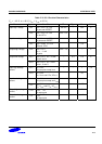
Supply current
(1)
I
DD1
(2)
V
DD
= 4.5 V to 5.5V
RUN mode
12 MHz CPU clock
15 30
V
DD
= V
LVR
to 5.5 V
8 MHz CPU clock
–
4 10
I
DD2
V
DD
= 4.5 V to 5.5 V
Idle mode
12 MHz CPU clock
3.4 7
V
DD
= V
LVR
to 5.5 V
8 MHz CPU clock
1 2.5
mA
I
DD3
Sub operating: main-osc stop
V
DD
= V
LVR
to 3.3 V
32768 Hz crystal oscillator
– 100 150 uA
I
DD4
Sub idle mode: main-osc stop
V
DD
= V
LVR
to 3.3 V
32768 Hz crystal oscillator
– 90 140
I
DD5
V
DD
= 4.5 V to 5.5 V,
T
A
= 25°C
Stop mode
– 80 100
V
DD
= V
LVR
to 3.3 V,
T
A
= 25°C
Stop mode
– 45 80
NOTES:
1. Supply current does not include current drawn through internal pull-up resistors or external output current loads.
2. I
DD1
and I
DD2
include a power consumption of subsystem oscillator.
3. I
DD3
and I
DD4
are the current when the main system clock oscillation stop and the subsystem clock is used.
4. I
DD5
is the current when the main and subsystem clock oscillation stop.
5. All currents (I
DD1
– I
DD5
) include the current consumption of LVR circuit.