


S3C84E5/C84E9/P84E9 ELECTRICAL DATA
17-7
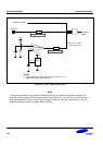
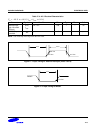
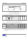
X
IN
t
XH
t
XL
1/f
OSC1
V
DD
- 0.5 V
0.4 V
Figure 17-3. Clock Timing Measurement at X
IN
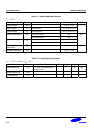
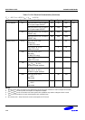
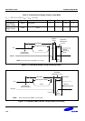
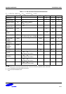
Table 17-7. Sub Oscillator Frequency (f
OSC2
)
(T
A
= –25
°
C + 85
°
C, V
DD
= V
LVR
to 5.5 V)
Oscillator Clock Circuit Test Condition Min Typ. Max Unit
Crystal
C1 C2
XT
IN
XT
OUT
R
Crystal oscillation frequency
C1 = 100 pF, C2 = 100 pF
R = 330 Ω
XT
IN
and XT
OUT
are connected
with R and C by soldering.
32 32.768 34 kHz
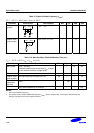
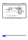
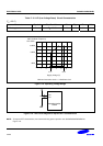
Table 17-8. Subsystem Oscillator (crystal) Stabilization Time (t
ST2
)
(T
A
= 25
°
C)
Oscillator Test Condition Min Typ. Max Unit
Normal mode
V
DD
= 4.5 V to 5.5 V
– 800 1600 ms
V
DD
= V
LVR
to 3.3 V
– 10 s
Strong mode
V
DD
= 4.5 V to 5.5 V
– 400 800 ms
V
DD
= V
LVR
to 3.3 V
– 150 300
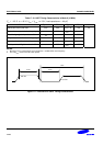
NOTE: Oscillation stabilization time (t
ST2
) is the time required for the oscillator to it's normal oscillation when stop mode
is released by interrupts. The value Typ. and Max are measured by buzzer output signal after stop release.
For example in voltage range of 4.5 V to 5.5 V of normal mode, we can see the buzzer output signal within 400 ms
at our test condition.