


A/D CONVERTER S3C84E5/C84E9/P84E9
15-4
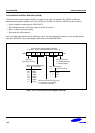
INTERNAL REFERENCE VOLTAGE LEVELS
In the ADC function block, the analog input voltage level is compared to the reference voltage. The analog input level
must remain within the range AVSS to AVREF (AVREF
= VDD).
Different reference voltage levels are generated internally along the resistor tree during the analog conversion process
for each conversion step. The reference voltage level for the first bit conversion is always 1/2 AVREF.
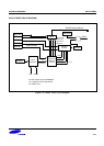
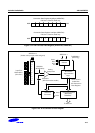
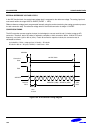
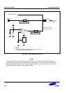
CONVERSION TIMING
The A/D conversion process requires 4 steps (4 clock edges) to convert each bit and 10 clocks to step-up A/D
conversion. Therefore, total of 50 clocks is required to complete a 10-bit conversion: With a 10 MHz CPU clock
frequency, one clock cycle is 400 ns (4/fxx). If each bit conversion requires 4 clocks, the conversion rate is
calculated as follows:
4 clocks/bit x 10-bits + step-up time (10 clock) = 50 clocks
50 clock x 400 ns = 20 µs at 10 MHz, 1 clock time = 4/fxx
50 ADC Clock
ADCON.0
. .
.
40 Clock
Previous
Value
Valid
Data
Set up
time
10 clock
ADDATAH (8-Bit) + ADDATAL (2-Bit)
9 8 7 6 5 4 3 2 1 0
Conversion
Start
EOC
ADDATA
Figure 15-4. A/D Converter Timing Diagram