


intJ
80386
5.
FUNCTIONAL DATA
5.1
INTRODUCTION
The 80386 features a straightforward functional in-
terface to the external hardware. The 80386 has
separate, parallel buses for data and address. The
data bus is 32-bits
in
width,
and
bidirectional. The
address
bus
outputs 32-bit address values
in
the
most directly usable form for the high-speed local
bus:
4 individual byte enable signals, and the
30
up-
per-order bits
as
a binary value. The data and
ad-
dress buses are interpreted and controlled with their
associated control signals.
A dynamic data bus sizing feature allows the proc-
essor to handle a
mix
of 32-
and
16-bit external
bus-
es
on
a cycle-by-cycle basis
(see
5.3.4 Data Bus
Sizing). If 16-bit bus size is selected, the 80386
au-
tomatically makes any adjustment needed, even
performing another 16-bit
bus
cycle to complete the
transfer if that is necessary. 8-bit peripheral devices
may be connected to 32-bit or 16-bit buses with no
loss of performance. A new address pipelining
op·
tion
is
provided and applies to 32-bit
and
16-bit bus-
es
for substantially improved memory utilization, es-
pecially for the most heavily used memory resourc-
es.
The address pipelining option, when selected, typ-
ically allows a given memory interface to operate
with one less wait state than would otherwise be
required (see 5.4.2 Address Pipelining). The pipe-
lined bus
is
also well suited to interleaved memory
designs. For 16
MHz
interleaved memory designs
with 100 ns access time DRAMs, zero wait states
can
be
achieved when pipe lined addressing is se-
lected. When address pipelining
is
requested by the
external hardware, the 80386 will output the address
and
bus
cycle definition of the next bus cycle (if it
is
internally available) even while waiting for the cur-
rent cycle to be acknowledged.
Non-pipelined address timing, however,
is
ideal for
external cache designs, since the cache memory will
typically be fast enough to allow non-pipelined cy-
cles. For maximum design flexibility, the address
pipelining option
is
selectable
on
a cycle-by-cycle
basis.
The processor's bus cycle
is
the basic mechanism
for information transfer, either from system to proc-
essor, or from processor to system.
80386 bus cy-
cles perform data transfer
in
a minimum of only two
clock periods.
On
a 32-bit data
bus,
the maximum
80386 transfer bandwidth at 16
MHz
is
therefore
32
Mbytes/sec. Any bus cycle will be extended for
more than two clock periods, however, if external
hardware withholds acknowledgement of the cycle.
60
At the appropriate time, acknowledgement
is
sig-
nalled
by
asserting the 80386 READY # input.
The 80386 can relinquish control of its local buses
to allow mastership by other devices, such
as
direct
memory access channels. When relinquished, HLDA
is
the only output
pin
driven
by
the 80386, providing
near-complete isolation of the processor from its
system. The near-complete isolation characteristic
is
ideal when driving the system from test equipment,
and
in
fault-tolerant applications.
Functional data covered
in
this chapter describes
the processor's hardware interface. First, the set of
signals available at the processor pins
is
described
(see
5.2
Signal Description). Following that are the
signal waveforms occurring during bus cycles (see
5.3
Bus Transfer Mechanism,
5.4
Bus Functional
Description and
5.5
Other Functional Descrip-
tions).
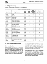
5.2
SIGNAL DESCRIPTION
5.2.1
Introduction
Ahead
is
a brief description of the 80386 input
and
output signals arranged by functional groups. Note
the
# symbol at the end of a signal name indicates
the active, or asserted, state occurs when the signal
is
at a low Voltage. When no #
is
present after the
signal
name,
the signal is asserted when at the high
voltage level.
Example signal:
M/IO#
- High voltage indicates
Memory selected
- Low voltage indicates
1/0
selected
The signal descriptions sometimes refer to
AC
tim-
ing
parameters, such
as
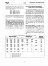
"t25 Reset Setup Time" and
"t26 Reset Hold Time." The values of these parame-
ters can be found
in
Tables 7-4 and 7-5.
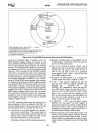
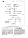
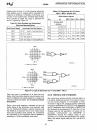
5.2.2 Clock (CLK2)
CLK2 provides the fundamental timing for the
80386. It is divided
by
two internally to generate the
internal processor clock used for instruction execu-
tion. The internal clock is comprised of two phases,
"phase one" and "phase two." Each CLK2 period
is
a phase of the internal clock. Figure
5-2
illustrates
the relationship. If desired, the phase of the internal
processor clock can be synchronized to a known
phase by ensuring the RESET signal falling edge
meets its applicable setup and hold times,
t25
and
t26·