


inter
80386
~[Q)W~OO~[g
OOOIP@OO~~lf'O@OO
6. MECHANICAL DATA
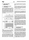
vee
and GND connections must be made to multi-
ple
Vee and Vss
(GND)
pins. Each Vee and Vss
must be connected to the appropriate voltage level.
6.1 INTRODUCTION
The circuit board should include Vee and
GND
planes for power distribution and all Vee and Vss
In
this section, the physical packaging and its con-
pins must
be
connected
to
the appropriate plane.
nections are described
in
detail.
NOTE:
Pins
identified as "N.C." should remain completely
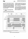
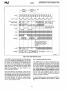
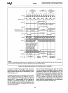
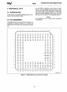
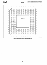
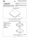
6.2 PIN ASSIGNMENT
unconnected.
The
80386 pinout as viewed from the top side of the
component
is
shown by Figure 6-1. Its pinout as
viewed from the
Pin
side of the component is Figure
6-2.
p
N
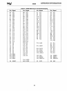
M L K H G D C B A
A30 A27
A26 A23
A21
A20 A17
A16
A15 A14
All
A8
VSS
vee
2
.... ....
2
vec
A31
A29
A24
A22
VSS
AlB
vee
VSS
A13
Al0
A7 A5
VSS
3
3
030
VSS
vec
A28 A25
VSS A19
vee
VSS
A12
A9 A6 A4 A3
4
4
029
vee
VSS
A2
NC
Ne
5
5
026
027
031
vee
VSS
vce
6
6
VSS
025
028
NC
Ne
VSS
7
7
024
VCC
vec
NC
INTR
vce
8
8
vcc
023
VSS
PEREQ
NMI
ERROR#
9
~ ~
9
.... ....
022
021
020
RESET
8USY#
VSS
10
10
019
017
VSS
LOCK#
W/R#
VCC
11
11
018 016
015
VSS
VSS
o/c#
12
~
~
~
~ ~
~
~
12
....
.... .... .... .... .... ....
014
012
010
vec
07
VSS
00
vec
CLK2
8EO#
vcc
vce
NC
M/IO#
13
13
013
011
VCC
08
05
VSS
01
REAOY#
Ne
NC
NA#
8El#
8E2# 8E3#
14
14
VSS
09
HLOA
06
04
03 02
VCC
VSS
AOS#
HOLO
8S16#
VSS
vcc
P N M
L K H G E D C B A
231630-33
Figure 6-1. 80386
PGA
Pinout-View
from Top Side
94