


266
Appendix 2 Details of Buffer Memory Addresses
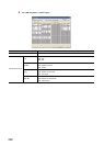
This section describes the buffer memory of the master/local module.
Appendix 2.1 Link device area (buffer memory address: 0 to
18975 (0
H
to 4A1F
H
))
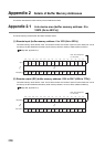
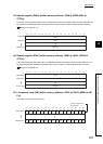
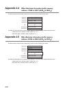
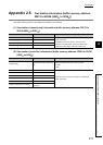
This buffer memory stores the RX, RY, RWw, and RWr values.
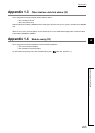
(1) Remote input (buffer memory address: 0 to 1023 (0
H
to 3EF
H
))
This buffer memory stores the RX value. The RX start number and number of points for each station No. can be
checked by the RX offset/size information (buffer memory address: 19456 to 19695 (4C00
H
to 4CEF
H
).
( Page 269, Appendix 2.2)
(2) Remote output (RY) (buffer memory address: 1024 to 2047 (400
H
to 7FF
H
))
This buffer memory stores the RY value. The RY start number and number of points for each station No. can be
checked by the RY offset/size information (buffer memory address: 19712 to 19951 (4D00
H
to 4DEF
H
)).
( Page 269, Appendix 2.3)
RX
3FFF
RX
3FFE
RX
3FFD
RX
3FFC
RX
3FFB
RX
3FFA
RX
3FF9
RX
3FF8
RX
3FF7
RX
3FF6
RX
3FF5
RX
3FF4
RX
3FF3
RX
3FF2
RX
3FF1
RX
3FF0
RX
F
RX
E
RX
D
RX
C
RX
B
RX
A
RX
9
RX
8
RX
7
RX
6
RX
5
RX
4
RX
3
RX
2
RX
1
RX
0
b0b1b2b3b4b5b6b7b8b9b10b11b12b13b14b15
Each bit corresponds
to 1 bit of RX.
1023(3FF
H)
0(0
H)
RY
3FFF
RY
3FFE
RY
3FFD
RY
3FFC
RY
3FFB
RY
3FFA
RY
3FF9
RY
3FF8
RY
3FF7
RY
3FF6
RY
3FF5
RY
3FF4
RY
3FF3
RY
3FF2
RY
3FF1
RY
3FF0
RY
F
RY
E
RY
D
RY
C
RY
B
RY
A
RY
9
RY
8
RY
7
RY
6
RY
5
RY
4
RY
3
RY
2
RY
1
RY
0
b0b1b2b3b4b5b6b7b8b9b10b11b12b13b14b15
Each bit corresponds
to 1 bit of RY.
2047(7FF
H)
1024(400
H)