


VX4101A MultiPaq Instrument User Manual
C–1
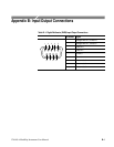
Appendix C: Instrument I/O Operation
CAUTION. If the user’s mainframe has other manufacturers’ computer boards
operating in the role of VXIbus foreign devices, the assertion of BERR* (as
defined by the VXIbus Specification) may cause operating problems on these
boards.
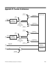
This section describes the input and output operations of the VX4101A
MultiPaqtInstrument. The VX4101A supports the Normal Transfer Mode of the
VXIbus using the Write Ready, Read Ready, Data In Ready (DIR), and Data Out
Ready (DOR) bits of the module Response register. The read and write opera-
tions in Normal Transfer Mode are as follows:
A Normal Transfer Mode read of the VX4101A Module proceeds as follows:
1. The commander reads the VX4101A Response register and checks if the
Write Ready and DOR bits are true. If they are, the commander proceeds to
the next step. If not, the commander continues to poll these bits until they
become true.
2. The commander writes the Byte Request command (hexadecimal 0DEFF) to
the Data Low register of the VX4101A.
3. The commander reads the VX4101A Response register and checks if the
Read Ready bit is true. If it is, the commander proceeds to the next step. If
not, the commander continues to poll this bit until it becomes true.
4. The commander reads the VX4101A Data Low register.
A Normal Transfer Mode write to the VX4101A Module proceeds as follows:
1. The commander reads the VX4101A Response register and checks if the
Write Ready and DIR bits are true. If they are, the commander proceeds to
the next step. If not, the commander continues to poll the Write Ready and
DIR bits until they are true.
2. The commander writes the Byte Available command which contains the data
(hexadecimal 0BCXX or 0BDXX, depending on the End bit) to the Data
Low register of the VX4101A.
The module has no registers beyond those defined for VXIbus message based
devices. All communications with the module are through the Data Low register,
the Response register, or the VXIbus interrupt cycle. Any attempt by another
module to read or write to any undefined location of the VX4101A address space
may cause incorrect operation of the module.
Normal Transfer Mode
Read Operation
Normal Transfer Mode
Write Operation