


www.digi.com
87
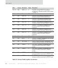
Memory Controller Module
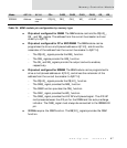
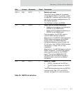
Chip select configured for SRAM. The MEM module controls the CS[4:0]_,
OE_, and WE_ signals. The address from the current bus master is driven
directly to A[27:0].
Chip select configured for FP or EDO DRAM. The MEM module can be
programmed to drive a multiplexed address on A[13:0], and drives the
remainder of the address from the current bus master to A[27:14].
– The CS[4:0]_ signals provide the RAS_ function.
– The CAS_ signals provide the CAS_ function.
– The OE_ and WE_ signals provide the output and write enables,
respectively.
Chip select configured for SDRAM. The MEM module can be programmed to
drive a multiplexed address on A[13:0], and drives the remainder of the
address from the current bus master to A[27:14].
– The CS[4:0]_ signals provide the CS[4:0]_ function.
– The CAS3_ signal provides the RAS_ function.
– The CAS2 function provides the CAS_ function.
– The CAS1_ signal provides the WE_ function.
– The CAS0_ signal provides the A10/AP multiplexed signal. The A10/AP
multiplexes between the A10 pin for the DRAM and the auto precharge
indicator. The CAS0_ signal must always be connected to the SDRAM A10
pin.
SDRAMs require the DQM function. The BE[3:0]_ signals provides the DQM
function.
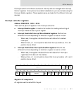
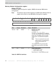
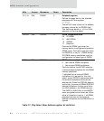
SDRAM Address Internal
mux
CS[4:0]_ RAS_ CAS_ WE_ A10/AP —— ——
Mode A27:14 A13:0 CSx CAS3_ CAS2_ CAS1_ CAS0_ OE_ WE_
Table 34: MEM module pin configuration by memory type