


Pinout detail tables and signal descriptions
24
NS7520 Hardware Reference, Rev. D 03/2006
System clock and reset
Signal descriptions
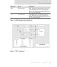
The NS7520 has three clock domains:
System clock (SYSCLK)
Bit rate generation and programmable timer reference clock (XTALA1/2)
System bus clock (BCLK)
The SYS module provides the NS7520 with these clocks, as well as system reset and
backup resources.
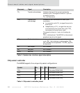
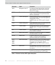
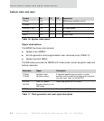
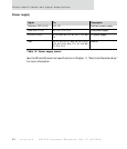
Symbol Pin I/O OD Description
XTALA1 K14 I ARM/system oscillator circuit
XTALA2 K12 O
PLLVDD (1.5V) L15 P PLL clean power
PLLVSS L12 P PLL return
RESET_ A10 I System reset
Table 10: System clock pinout
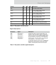
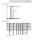
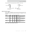
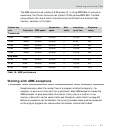
Mnemonic Signal Description
XTALA1
XTALA2
Oscillator input
Oscillator output
A standard parallel quartz crystal or crystal
oscillator can be attached to these pins to provide
the main input clock to the NS7520.
PLLVDD
PLLVSS
Clean PLL power
Connect directly to the
GND plane
Power and ground for PLL circuit.
RESET_ System reset Resets the NS7520 hardware.
Table 11: Clock generation and reset signal description