


Signal description
48
NS7520 Hardware Reference, Rev. D 03/2006
Signal description
The system control signals determine the basic operation of the chip:
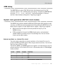
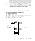
JTAG support
The NS7520 provides full support for 1149.1 JTAG boundary scan testing. All NS7520
pins can be controlled using the JTAG interface port. The JTAG interface provides
access to the ARM7TDMI debug module when the appropriate combination of PLLTST_,
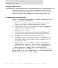
BISTEN_, and SCANEN_ are selected (see "External oscillator mode hardware
configuration," beginning on page 51).
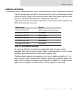
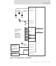
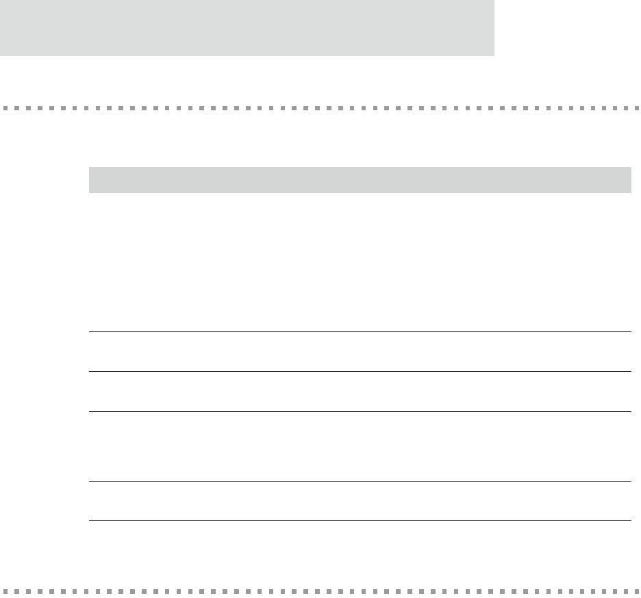
Signal mnemonic Signal name Description
{XTALA1, XTALA2} Clock source Operate in one of two ways:
The signals are affixed with a 10-20
MHz parallel mode quartz crystal or
crystal oscillator and the appropriate
components per the component
manufacturer.
XTALA1 is driven with a clock signal
and XTALA2 is left open.
{PLLVDD, PLLVSS} PLL power Provide an isolated power supply for the
PLL.
RESET_ Chip reset Active low signal asserted to initiate a
hardware reset of the chip.
{TDI, TDO, TNS,
TRST_, TCK}
JTAG interface Provide a JTAG interface for the chip.
This interface is used for both boundary
scan and ICE control of the internal
processor.
{PLLTEST_, BISTEN_,
SCANEN_}
Chip mode Encoded to determine the chip mode.