


www.digi.com
15
Pinout and Packaging
Signal descriptions
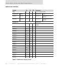
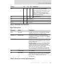
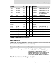
TEA_ C8 U I/O 4 Data transfer error acknowledge
Add an external 820 ohm pullup to 3.3 V.
TEA_ is bidirectional. It is used in input
mode to terminate a memory cycle
externally. It is used in output mode for
reference purposes only.
RW_ D6 I/O 2 Transfer direction
BR_ D7 NO CONNECT
BG_ C7 NO CONNECT
BUSY_ B7 NO CONNECT
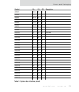
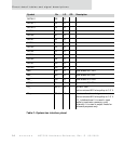
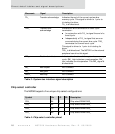
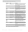
Mnemonic Signal Description
BCLK Bus clock Provides the bus clock. All system bus interface
signals are referenced to the BCLK signal.
ADDR[27:0] Address bus Identifies the address of the peripheral being
addressed by the current bus master. The address
bus is bi-directional.
DATA[31:0] Data bus Provides the data transfer path between the
NS7520 and external peripheral devices. The data
bus is bi-directional.
Recommendation: Less than x32 (S)DRAM/SRAM
memory configurations. Unconnected data bus
pins will float during memory read cycles. Floating
inputs can be a source of wasted power.
For other than x32 DRAM/SRAM configurations,
the unused data bus signals should be pulled up.
TS_ Transfer start NO CONNECT
BE_ Byte enable Identifies which 8-bit bytes of the 32-bit data bus
are active during any given system bus memory
cycle. The BE_ signals are active low and
bi-directional.
Table 3: System bus interface signal description
Symbol Pin I/O OD Description
Table 2: System bus interface pinout