


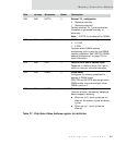
www.digi.com
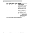
103
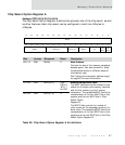
Memory Controller Module
Single cycle read/write
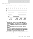
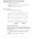
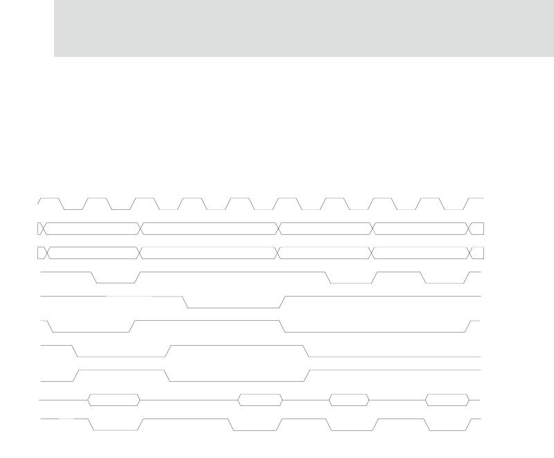
Synchronous SRAM cycles are used primarily for peripherals that can use BCLK or
CS[4:0]_ as the data transfer signal. Figure 6 shows synchronous SRAM cycles.
Figure 6: Synchronous SRAM cycles
All outputs change state relative to the rising edge of BCLK with the
exception of OE_ and WE_, which transition on the falling edge of BCLK.
The OE_ and WE_ signals change state on the falling edge before CS[4:0]_ is
asserted.
OE_ and WE_ remain active until the falling edge after CS[4:0]_ is
deasserted.
The rising edge of BCLK where TA_ is low defines the end of the memory
cycle (referred to as the T2 state). During synchronous read cycles, read
data is sampled on the rising edge of BCLK where TA_ is low.
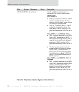
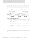
Asynchronous SRAM cycles guarantee that the WE_ and OE_ pulses are inside the
active low pulse of CS[4:0]_. Asynchronous SRAM cycles operate a minimum of 1 wait
state at all times. Figure 7 shows asynchronous SRAM cycles.
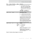
Sync Write Sync Read
Sync Write Sync Write
BCLK
ADDR
BEn_
CS0_
CS1_
R/W_
WE_
OE_
DATA
TA_
T1 T2 T1 TW T2 T1 T2 T1 T2