


www.digi.com
255
Serial Controller Module
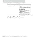
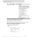
Reading to this register empties the receive FIFO. Data is available when the RRDY bit
is set in Serial Channel Status Register A. The RXFDB bits in Serial Channel Status
Register A indicate how many bytes are available to be read. Reading the Serial
Channel FIFO register automatically clears the RRDY bit.
Register bit assignment
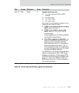
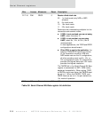
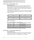
Serial Channel 1, 2 Receive Buffer Gap Timer
Address: FFD0 0014 / 54
The Receive Buffer Gap Timer register closes out a receive serial data buffer. The
timer is reset when the first character is received in a new buffer. New characters
are received while the timer operates. When the timer reaches its programmed
threshold, the receive data buffer is closed.
If the serial channel is configured to operate in DMA mode, the DMA channel is
signaled to close the buffer and start a new buffer. If the serial channel is configured
to operate in interrupt mode, the expiration of the timer causes an interrupt to be
generated.
The receive buffer timer uses F
XTALE
and a 9-bit prescaler within the SER module. The
receive buffer timer is configured with a 15-bit programmable counter. The effective
buffer timer value is defined by this equation:
TIMEOUT = [512 * (BT + 1)] / F
XTALE
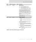
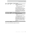
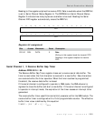
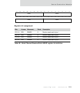
Bits Access Mnemonic Reset Description
D31:00 R/W DATA 0 Data
Writing to this register loads the transmit FIFO
Reading to this register empties the receive
FIFO.
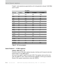
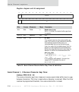
13121110987654321015 14
31 29 28 27 26 25 24 23 22 21 20 19 18 17 1630
DATA
DATA