


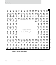
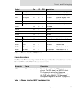
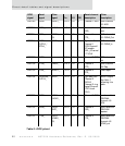

Pinout detail tables and signal descriptions
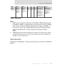
18
NS7520 Hardware Reference, Rev. D 03/2006
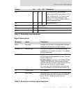
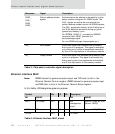
Ethernet interface MAC
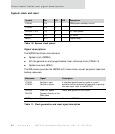
Note:
ENDEC values for general-purpose output and TXD refer to bits in the
Ethernet General Control register. ENDEC values for general-purpose input
and RXD refer to bits in the Ethernet General Status register.
In this table, GP designates general-purpose.
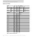
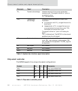
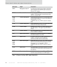
CAS0_
CAS1_
CAS2_
CAS3_
Column address strobe
signals
Activated when an address is decoded by a chip
select module configured for DRAM mode. The
CAS_ signals are active low and provide the
column address strobe function for DRAM devices.
The CAS_ signals also identify which 8-bit bytes of
the 32-bit data bus are active during any given
system bus memory cycle.
For SDRAM, CAS[3:1]_ provides the SDRAM
command field. CAS0_ provides the
auto-precharge signal.
For non-DRAM settings, these signals are 1.
WE_ Write enable Active low signal that indicates that a memory
write cycle is in progress. This signal is activated
only during write cycles to peripherals controlled
by one of the chip selects in the memory module.
OE_ Output enable Active low signal that indicates that a memory read
cycle is in progress. This signal is activated only
during read cycles from peripherals controlled by
one of the chip selects in the memory module.
Mnemonic Signal Description
Table 5: Chip select controller signal description
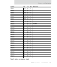
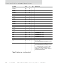
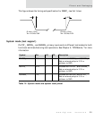
Symbol Pin I/O OD Description
MII ENDEC MII ENDEC
MDC GP output D10 O 2 MII
management
clock
State of (LPBK bit XOR
(Mode=SEEQ))
MDIO GP output B10 U I/O 2 MII data State of UTP_STP bit
TXCLK C10 I TX clock
Table 6: Ethernet interface MAC pinout