


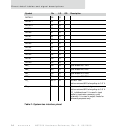
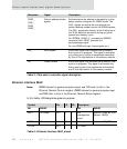
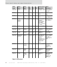
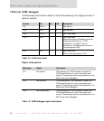
Pinout detail tables and signal descriptions
22
NS7520 Hardware Reference, Rev. D 03/2006
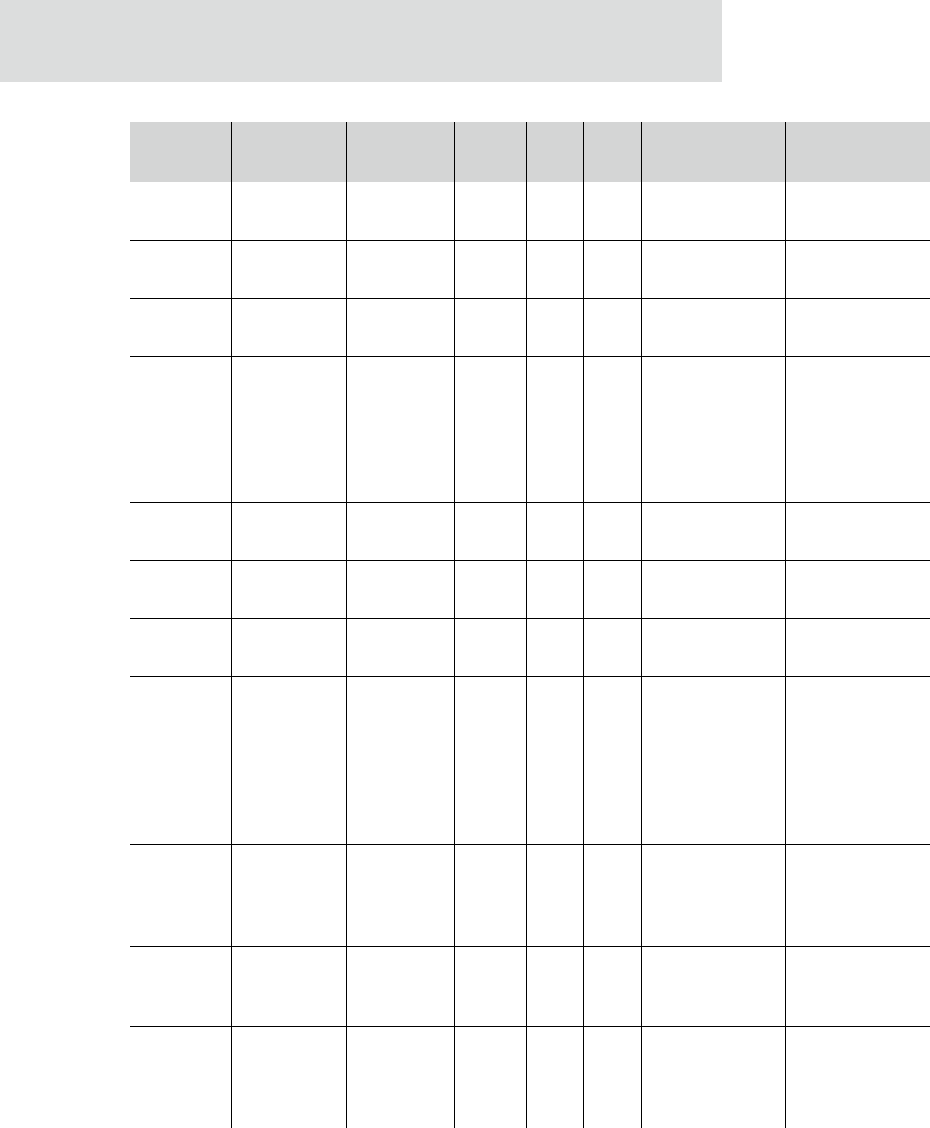
PORTA3 RXDA DACK1_ H15 U I/O 2 Channel 1 RXD DMA channel
3/5 ACK
PORTA2 DSRA_ AMUX H12 U I/O 2 Channel 1
DSR_
DRAM addr
mux
PORTA1 CTSA_ DONE1_
(O)
H13 U I/O 2 Channel 1
CTS_
DMA channel
3/5 DONE_Out
PORTA0 TXCA/
OUT2A_/
DCDA_
DONE1_ (I) G12 U I/O 2 Pgm’able Out/
Channel 1
DCD/Channel 1
SPI enable
(SEL_)/Channel
1 TXCLK
DMA channel
3/5 DONE_In
PORTC7 TXDB G13 U I/O 2 Channel 2 TXD GEN interrupt
out
PORTC6 DTRB_ DREQ2_ G14 U I/O 2 Channel 2
DTR_
DMA channel
4/6 Req
PORTC5 RTSB_ REJECT_ F15 U I/O 2 Channel 2
RTS_
CAM reject
PORTC4 RXCB/RIB_/
OUT1B_
RESET_ F12 U I/O 2 Pgm’able Out/
Channel 2
RXCLK/
Channel 2 ring
signal/Channel
2 SPI clock
(CLK)
RESET output
See Note 1
following this
table.
PORTC3
2
RXDB LIRQ3/
DACK2_
F13 U I/O 2 Channel 2 RXD Level sensitive
IRQ/DMA
channel 4/6
ACK
PORTC2
2
DSRB_ LIRQ2/
RSPF_
E15 U I/O 2 Channel 2
DSR_
Level sensitive
IRQ/CAM
request
PORTC1
2
CTSB_ LIRQ1/
DONE2_
(O)
E12 U I/O 2 Channel 2
CTS_
Level sensitive
IRQ/DMA
channel 4/6
DONE_out
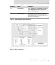
GPIO
signal
Serial
signal
Other
signal
Pin I/O OD
Serial channel
description
Other
description
Table 9: GPIO pinout