


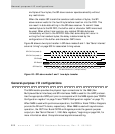
General-purpose I/O configurations
222
NS7520 Hardware Reference, Rev. D 03/2006
multiples of four bytes, the SPI slave receiver operates smoothly without
any restrictions.
When the master SPI transmitter sends an odd number of bytes, the SPI
slave receiver waits for the fourth byte before insertion into the FIFO. This
can result in stale data sitting in the SPI slave receiver. To commit these
residual bytes to the RX FIFO, the buffer and/or character GAP timers must
be used. When either timer expires, any residual RX data bytes are
immediately written to the RX FIFO. Note that some delay will occur in
writing the final residual bytes; the delay is determined by the
configuration of the buffer and character GAP timers.
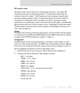
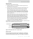
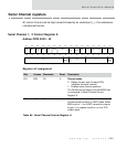
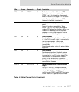
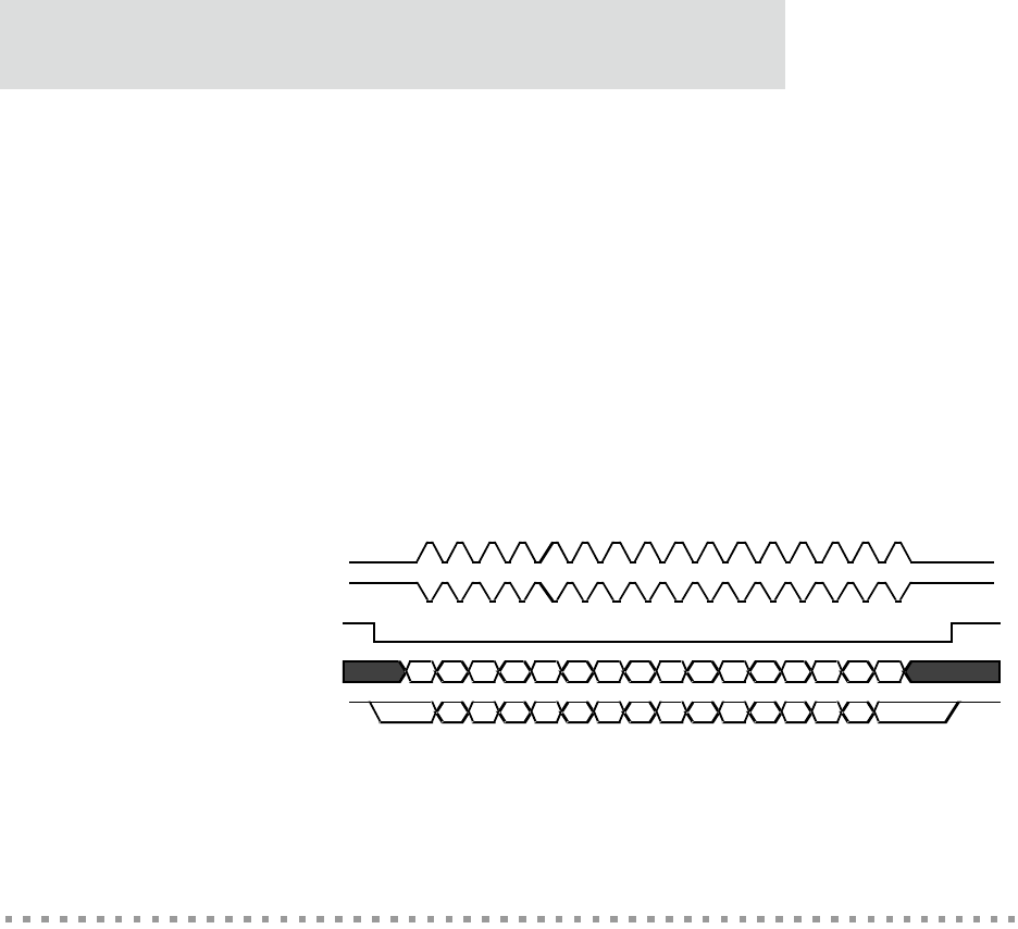
Figure 26 shows a two-byte transfer in SPI slave modes 0 and 1. See "Serial internal/
external timing" on page 303 for associated timing values.
Figure 26: SPI slave mode 0 and 1 two-byte transfer
General-purpose I/O configurations
The GEN module provides the physical layer connections for the NMSI (Non
Multiplexed Serial Interface) and SPI interfaces. NMSI is used for the UART protocol.
Use the appropriate GPIO port pins to correspond with the NMSI signals (see "PORTA
Configuration register" on page 74 and "PORTC Configuration register" on page 77).
When NMSI is used with synchronous operation, the RXCA or B and TXCA or B signals
provide the RX and TX clocks, respectively. When NMSI is used with asynchronous
operation, the OUT1A or B and OUT2A or B signals provide the general-purpose
output pin. See "Serial Channel 1, 2 Bit-Rate registers," beginning on page 244, for
more information about this synchronous/asynchronous setting.
SPI Slave Mode 0 and 1, (Two Byte Transfer)
msb lsb msb
lsb
msb
lsb msb
lsb
SPI CLK Out (mode 0)
SPI CLK Out (mode 1)
SPI Enable
SPI Data In
SPI Data Out