


GEN module registers
66
NS7520 Hardware Reference, Rev. D 03/2006
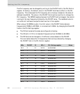
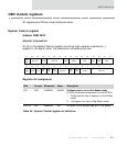
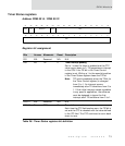
D14 R/W BUSER ~ADDR
[26]
Enable ARM CPU
Must be set to 0.
When reset, BUSER defaults to the value defined
by ADDR26 (see "NS7520 bootstrap
initialization" on page 60).
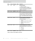
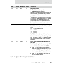
D13 N/A Reserved N/A N/A
D12 R/W DMATST 0 DMA module test mode
Resets the DMA controller subsystem. Also
allows the ARM processor direct access to the
internal context RAM found in the DMA controller.
When set to 1 (allow unrestricted access),
the DMA controller subsystem is held in reset
and the ARM processor can access all
internal DMA context RAM. This is useful for
diagnostic purposes.
When set to 0 (test mode disabled), the DMA
controller subsystem operates normally. Only
the bits in the DMA Control register space
can be accessed by the ARM processor.
D11 R/W TEALAST 0 Bus interface TEA/LAST configuration
This bit can be read or written with a setting of 1
or 0, but has no effect on chip functionality.
D10 R/W MISALIGN 0 Bus error on misaligned cycles
0 Disable misaligned data transfer bus abort
generation
1 Generate a bus abort during a misaligned
transfer
When this bit is set to 1, misaligned address
transfers cause a data abort to be issued to the
offending bus master. A misaligned address
transfer is defined as a half word access to an odd
byte address boundary, or a full word access to
either a half word or byte address boundary.
This bit is useful during software debugging to
detect misaligned cycles.
D09:08 N/A Reserved N/A N/A
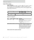
Bits Access Mnemonic Reset Description
Table 24: System Control register bit definition