


www.digi.com
111
Memory Controller Module
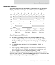
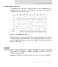
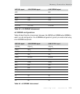
FP/EDO DRAM burst cycles
The DRAM controller supports both read and write burst cycles. A DRAM Burst cycle
must operate with a minimum of one wait state for the first cycle and a minimum of
two BCLK cycles in subsequent cycles.
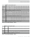
Figure 10: FP DRAM burst cycles
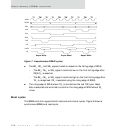
When bursting at full bus speed with EDO, write timing is controlled by a combination
of BCYC and WAIT; otherwise, BCYC controls the length of subsequent burst cycles.
(See "Chip Select Option Register A," beginning on page 97, for information about the
BCYC and WAIT fields.)
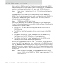
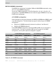
SDRAM
The DMODE field in the Chip Select Base Address register configures a chip select for
SDRAM (synchronous DRAM).
Important:
The NS7520 cannot perform 16-bit burst operations from an x32 SDRAM.
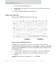
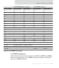
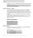
T1 TW T2 TW TWT2 TWT2 T2
BCLK
RAS_
ADDR
CAS_
WE_
OE_
TA_
TEA_
DATA Read
DATA Write