


www.digi.com
101
Memory Controller Module
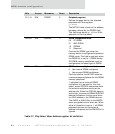
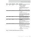
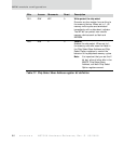
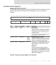
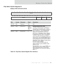
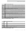
Chip Select Option Register B
Address: FFC0 0018/28/38/48/58
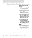
Bits Access Mnemonic Reset Description
D31:06 N/A Reserved N/A N/A
D05:04 R/W WAIT[5:4] 0 for
CS[4:1],
’b11 for
CS0
Memory timing control fields
The WAIT field controls the number of
wait states for all single cycle memory
transfers and the first memory cycle of a
burst transaction. The complete WAIT
field is the concatenation of the four
WAIT bits in Chip Select Option Register
A and the two WAIT bits in this register.
The BCYC field controls the number of
clock cycles for the secondary portion of
a burst cycle. The complete BCYC field is
the concatenation of the two BCYC bits in
Chip Select Option Register A and the two
BCYC bits in this register.
For OE- or WE-controlled cycles, an
additional BCLK cycle is added to each
memory cycle.
For information about related DRSEL and
DMODE settings, see the Chip Select
Option Register A bit definition table (on
page 97).
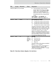
D03:02 R/W BCYC[3:2] 0
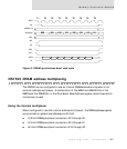
Table 39: Chip Select Option Register B bit definition
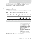
13121110987654321015 14
31 29 28 27 26 25 24 23 22 21 20 19 18 17 1630
Reserved
Reserved
WAIT[5:4] BCYC[3:2] SYNC