


www.digi.com
91
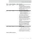
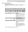
Memory Controller Module
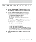
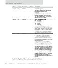
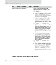
D22:21 R/W RCYC 0 Refresh cycle count
The refresh timing, based on the sample
timing diagram shown in "fp_refresh_cycles"
on page 294, is selected by the value in this
field for all chip selects programmed for FP/
EDO DRAM operation.
This field has no effect on SDRAM.
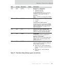
D20 R/W AMUX 0 Enable external address multiplexing
0 Disable external address multiplexing on
PORTA2 for all DRAM banks
1 Enable external address multiplexing on
PORTA2 for all DRAM banks
Controls whether the NS7520 uses its
internal DRAM address multiplexer.
When set to 0, the NS7520 uses the internal
DRAM address multiplexer for all DRAM
access cycles. The DRAM RAS/CAS
multiplexed address is routed through the
A13:A0 pins. See "NS7520 DRAM address
multiplexing" on page 105 for more
information.
When set to 1, the NS7520 uses an external
DRAM multiplexer. The RAS/CAS address
select signal is routed out the PORTA2
signal. The external DRAM RAS/CAS
multiplexer uses the PORTA2 signals to
determine when to switch the address
multiplexer
D19 R/W A[27] 0 Enable A27 output
0 CS0OE_ is driven out the A27 pin
1 The A27 signal is driven out the A27
pin
The bit settings determine how the NS7520
uses this signal. See "A27 and A26 bit
settings" on page 92 for more information.
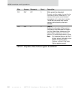
Bits Access Mnemonic Reset Description
Table 36: MMCR bit definition