


www.digi.com
95
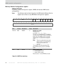
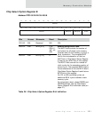
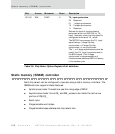
Memory Controller Module
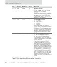
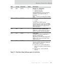
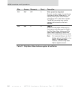
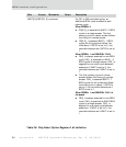
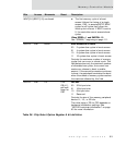
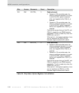
D06 R/W EXTTA 0 External TA_ configuration
0 Generate internally
1 Generate externally
Defines whether TA_ cycle termination
indication is generated internally or
externally.
Note: EXTTA is not allowed for DRAM.
D05 R/W DMUXM 0 DRAM internal address multiplexer mode
0 10 CAS
18 CAS
Controls which DRAM address
multiplexing style is used for this DRAM
memory peripheral. See "NS7520 DRAM
address multiplexing" on page 105 for
more information.
D04 R/W IDLE 0 Force BCLK at end of memory cycle
Responds to read and write, but has no
effect on memory controller operation.
D03 R/W DRSEL 0 DRAM select
Configures the memory peripheral to
operate in DRAM mode.
WE CTRL and OE CTRL bits are ignored in
DRAM mode; they are used only when
DRSEL is set to 0.
D02 R/W BURST 0 Burst memory cycle enable
Controls whether the memory peripheral
device supports bursting.
When set to 0, burst cycles are not
allowed. All memory cycles are single
cycles.
When set to 1, burst cycles are
allowed.
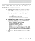
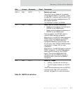
Bits Access Mnemonic Reset Description
Table 37: Chip Select Base Address register bit definition