


www.digi.com
303
Electrical Characteristics
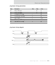
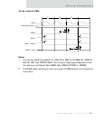
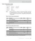
Serial internal/external timing
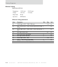
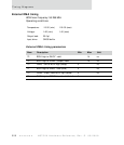
Operating conditions:
Note:
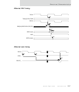
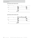
SPI timing diagrams are in Chapter 10, "Serial Controller Module." See Figure
25, "SPI master mode 0 and 1 two-byte transfer," on page 219 and Figure 26,
"SPI slave mode 0 and 1 two-byte transfer," on page 222. Only SPI modes 0 and
1 are supported.
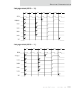
Serial internal timing characteristics
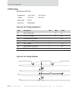
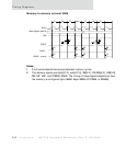
Serial external timing characteristics
Temperature: -15.00 (min) 110.00 (max)
Voltage: 1.60 (min) 1.40 (max)
Output load: 25.0pf
Input drive: CMOS buffer
Num Description Min Max Unit
76 SCLK to ENABLE high 1 T
SCLK
77 SCLK to TXD (PORTA7/C7) 1 T
SYS
*ns
78 RXD (PORTA3/C3) setup to SCLK 1 ns
79 RXD hold to SCLK 1 ns
* The T
SYS
parameter represents one period of the internal system clock.
Num Description Min Max Unit
80 SCLK frequency 10 MHz
SCLK duty cycle 45 55 %
81 SCLK to ENABLE 1 T
SCLK
82 SCLK to TXD (PORTA7/C7) 2T
SYS
*ns
83 RXD (PORTA3/C3) setup to SCLK 2 ns
84 RXD hold to SCLK 1.5 ns
* The T
SYS
parameter represents one period of the internal system clock.