


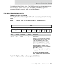
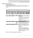

MEM module configuration
92
NS7520 Hardware Reference, Rev. D 03/2006
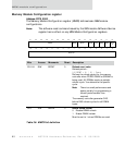
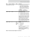
A27 and A26 bit settings
The A27 bit setting determines how the A27 signal is used by the NS7520. CS0OE_ is
generated by an internal logical AND of the CS0_ and OE_ signals. The CS0OE_ signal
goes active low when both CS0_ and OE_ are active low.
The A26 bit setting determines how the A26 signal is used by the NS7520. The CS0WE_
signal is generated by an internal logical AND of the CS0_ and WE_ signals. the
CS0WE_ signal goes active low when both CS0_ and WE_ are active low.
When enabled, these signals maximize the read access timing for external memory
peripherals attached to CS0. When using CS0OE_, the CS0 peripheral’s chip select
input is attached to GND, and the read-access time for that peripheral is referenced
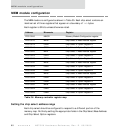
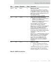
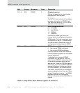
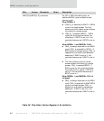
D18 R/W A[26] 0 Enable A26 output
0 CS0WE_ is driven out the A26 pin
1 The A26 signal is driven out the A26
pin.
The bit settings determine how the NS7520
uses this signal. See "A27 and A26 bit
settings" on page 92 for more information.
D17 R/W A25 1 Enable A25 output
Always set to 0; used for address bit 25.
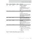
D16 R/W AMUX2 0 Internal/External/RAS/CAS mux
0 Normal operation
1 Drive the DRAM MUX control out
PORTA2, regardless of the AMUX and
DMUXS settings
Used to drive the DRAM RAS/CAS address
multiplexing control signal out the PORTA2
pin, regardless of the AMUX setting.
When set to 1, the memory controller drives
the DRAM RAS/CAS address multiplexing
control signal out the PORTA2 pin, for an
external address multiplexer to use for
DRAM RAS/CAS address multiplexing
control.
D15:00 N/A Reserved N/A N/A
Bits Access Mnemonic Reset Description
Table 36: MMCR bit definition