


www.digi.com
117
Memory Controller Module
The NS7520 provides the A10/AP multiplexing function using the CAS0_ pin. During
the active command, the CAS0_ pin is driven with the logical value of one of the
address bits A[21:18] as a function of the port size configuration defined in Chip
Select Option Register A and the mux mode defined in the Chip Select Base Address
register.
This table defines which address bit is driven in each situation:
During the read or write commands, the NS7520 drives a 0 on the CAS0_ pin
(indicating that automatic precharge should not be performed). During the precharge
command, the NS7520 drives a 1 on the CAS0_ pin (indicating that all banks should be
precharged.)
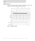
Command definitions
SDRAMs operate according to a series of command codes that are issued while chip
select input is active low. The command codes are registered using the low-to-high
transition of the synchronous clock. NS7520 implementation requires that all SDRAMs
are synchronized to the NS7520 BCLK signal.
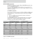
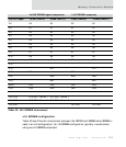
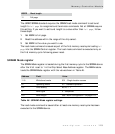
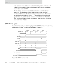
Mux mode x32 x16 x8
0 201918
1 212019
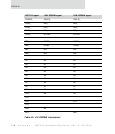
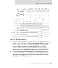
Command
CSx_ A13:0 CAS3_ RAS# CAS2_ CAS# CAS1_ WE# CAS0_ A10/AP
Inhibit 1 X X X X X
NOP 0 X 1 1 1 X
Active 0 Bank/row 0 1 1 A10
Read 0 Column 1 0 1 0
Write 0 Column 1 0 0 0
Burst Term 0 X 1 1 0 X
Precharge 0 X 1 1 0 X
Refresh 0 X 0 0 1 X
Table 45: SDRAM command definitions