


www.digi.com
219
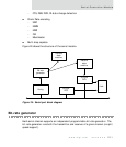
Serial Controller Module
SPI master receiver
The SPI master receiver operates as follows:
Samples the RXD input on the rising edge of the SPI clock signal while the
SPI enable signal is driven active low.
Receives one byte of inbound data for each byte of transmit data sent. The
SPI master receiver cannot receive more data that what is transmitted.
When the SPI master receiver collects four bytes, those four bytes are
written to the RX FIFO. Receive data is read by the CPU or DMA controller
from the other side of the FIFO. If the SPI master transmitter always sends
data in multiples of four bytes, the SPI master receiver operates smoothly
without any restrictions.
When the SPI master transmitter sends an odd number of bytes, the SPI
master receiver needs to wait for the fourth byte before insertion into the
FIFO. This can result in stale data sitting in the SPI master receiver. To
commit these residual bytes to the RX FIFO, the buffer and/or character
GAP timers must be used. When either timer expires, any residual RX data
bytes are immediately written to the RX FIFO. Note that some delay will
occur in writing the final residual bytes; the delay is determined by the
configuration of the buffer and character GAP timers.
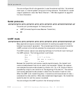
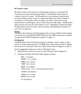
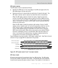
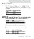
Figure 25 shows a two-byte transfer in SPI master modes 0 and 1. See "Serial internal/
external timing" on page 303 for associated timing values.
Figure 25: SPI master mode 0 and 1 two-byte transfer
SPI slave mode
SPI slave mode supports the peripheral side of an SPI interface. The SPI master
controls the number of bytes for the transfer. The SPI slave port simultaneously
transmits and receives the same number of bytes. The transfer of information is
SPI Master Mode 0 and 1, (Two Byte Transfer)
msb lsb msb
lsb
msb
lsb msb
lsb
SPI CLK Out (mode 0)
SPI CLK Out (mode 1)
SPI Enable
SPI Data In
SPI Data Out