


AC characteristics
266
NS7520 Hardware Reference, Rev. D 03/2006
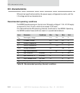
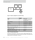
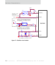
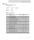
Figure 30: System configuration for specified timing
Exceeding the loading shown in Table 100 can result in additional signal delay. The
delay can be approximated by derating the output buffer based on the expected load
capacitance per the values shown in Table 101.
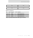
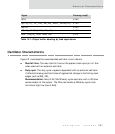
Signal
Estimated
load (pF) Device loads
BCLK 23 Two SDRAMs, 1 clock buffer/
clock input to PLD
A[27:0], CAS[3:0]_ 23 Two SDRAM An, 1 buffer/PLD
CS[4:0]_ 13 Two SDRAM CSn, 1 buffer PLD
DATA[31:0] 18 One SDRAM DQ, 1 buffer/PLD
BE*_ 19 One SDRAM DQ, 1 buffer/PLD
TS_, TA_, TEA_, BR_, BG_, BUSY_, WE_,
OE_
15 1 buffer/PLD
PORTA3, PORTA1, PORTC3, PORTC1
(operating external DMA)
15 1 buffer/PLD
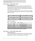
Other PORTA[*] and PORTC[*], TDO 85 Tester load
MDC, MDIO, TXEN, TXER, TXD[3:0] 20 One PHY
Table 100: System loading details
SDRAM SDRAM
NS7520
other
memory
devices
Buffer