


Using the PLL circuit
52
NS7520 Hardware Reference, Rev. D 03/2006
Using the PLL circuit
The NS7520 can use its PLL external oscillator to generate the BCLK and FXTAL
signals. In this configuration, BCLK can be set to several values, in increments of 1/4
the crystal frequency. FXTAL us always the crystal frequency divided by five.
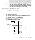
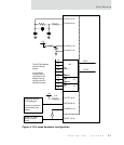
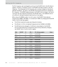
PLL mode hardware configuration
Figure 5, "PLL mode hardware configuration," on page 53, shows how the crystal is
connected to the XTALA1 and XTALA2 inputs.
When the clock module is configured to use the PLL, the power to the
module must be cleaner than when using an external oscillator.
PLLVDD must be connected to 1.5V through a ferrite bead and bypassed with
a 100nF capacitor placed close to ball L15.
PLLVSS is connected to ground.
The PLLTST input i s connected to ground to use the JTAG debugger; it is
connected to 3.3V through a 10K resistor to use boundary scan testing.
The BISTEN* input is tied to 3.3 volts through a 10K resistor.
The SCANEN* must be low to choose the PLL mode. The SCANEN* input must
be connected to system reset through an inverter, to ensure that the PLL
circuit is properly reset.
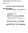
RESET* must have a rise time of 18nS from 0.8V to 2.0V. The MAX811 is in
this range. A RESET* source with a slow rise time can be used by using a
double inverter. The first inverter’s output connects to SCANEN* and to the
second inverter input. The second inverter’s output drives RESET*.
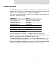
Address lines A[8:0] configure the PLL circuit on bootup. Note that the values on
address lines A8, A6, A5, A4, and A2 are inverted in the PLL Settings register (see
"Setting the PLL frequency," beginning on page 54).