


www.digi.com
89
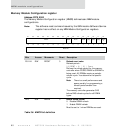
Memory Controller Module
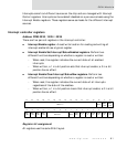
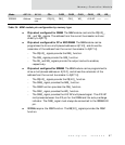
The BASE field in the Chip Select Base Address register defines the starting address of
the chip select address space. The MASK field identifies those address bits, from
A[31:12], that are used in the address decoding function.
A 1 in the MASK field indicates that the associated address bit is to be used
in the decoding process.
A 0 in the MASK field indicates that the associated address is to be ignored
in the address decoding process.
Note:
When accessing a static memory device, the maximum value of the base
address is
0x03000000.
To determine whether a BBus address is associated with a peripheral chip select,
apply the following Boolean equation (chip select decode is TRUE when):
(({MASK,000} & 32-bit logical address) = = ({BASE,000} & {MASK,000}))
{MASK,000} is the MASK field concatenated with three nibbles of 0.
{BASE,000} is the BASE field concatenated with three nibbles of 0.
& is the logical AND function.
== is the equal to operator.
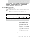
The NS7520 supports only 28 address bits. Each chip select is limited to 256 Mbytes.
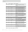
Memory Space
The MASK field can alias a memory location in different areas. The memory space
associated with an individual chip select does not have to be continuous. Using the
MASK field, you can set gaps in a single chip select range, essentially assigning the
same chip select to different portions of the memory map.
Example
A 16 Mbyte device can be addressed in four different 64 Mbyte address locations by
using a MASK value of
’hF3000. The peripheral is addressable at these address
locations:
BASE + ’h00000000
BASE + ’h04000000
BASE + ’h08000000
BASE + ‘h0C000000