


www.digi.com
97
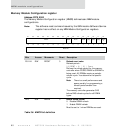
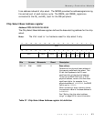
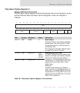
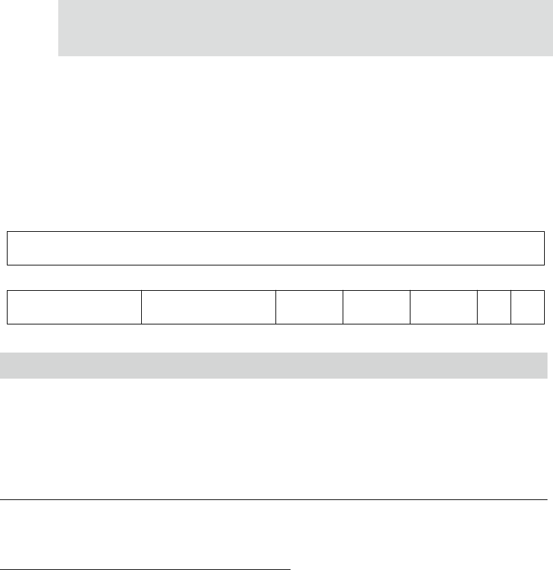
Memory Controller Module
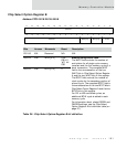
Chip Select Option Register A
Address: FFC0 0014/24/34/44/54
The Chip Select Option Register A defines the physical size of the chip select, as well
as other features. Each chip select can be configured in size from 4 Kbytes to
4 Gbytes.
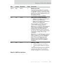
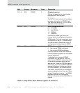
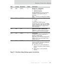
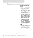
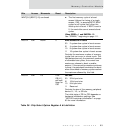
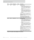
Bits Access Mnemonic Reset Description
D31:12 R/W MASK 0 Mask Address
Controls the size of the memory peripheral
decode space. Can also be used to “alias”
the peripheral device in different areas of
the memory map.
See "Setting the chip select address range"
on page 88 for more information.
D11:08 R/W WAIT[3:0] 0 for
CS[4:1],
‘b1111
for CS0
Memory timing control fields
The WAIT field controls the number of wait
states for all single cycle memory transfers
and the first memory cycle of a burst
transaction. The complete WAIT field is the
concatenation of the four WAIT bits in this
register and the two WAIT bits in Chip
Select Option
Register B.
The BCYC field controls the number of
clock cycles for the secondary portion of a
burst cycle. The complete BCYC field is the
concatenation of the two BCYC bits in this
register and the two BCYC bits in the Chip
Select Option Register B.
D07:06 R/W BCYC[1:0] 0
Table 38: Chip Select Option Register A bit definition
13121110987654321015 14
31 29 28 27 26 25 24 23 22 21 20 19 18 17 1630
MASK
MASK WAIT[3:0] BCYC[1:0] BSIZE PS
OE
CTRL_
WE
CTRL_