www.digi.com
67
GEN Module
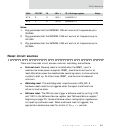
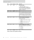
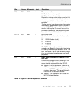
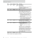
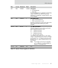
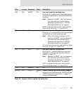
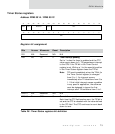
D07 R/W CPUDIS
-ADDR26
CPU disable
0 CPU operational
1CPU reset
Provides a mechanism to read back the bootstrap
value of ADDR26 (see "NS7520 bootstrap
initialization" on page 60). If this bit is set to 1, the
CPU is disabled.
D06 R/W DMARST 0 DMA module reset
0 DMA module operational
1 DMA module (held in) reset
Provides a mechanism to issue a soft reset to the
DMA module without affecting any other
modules.
D05:04 R/W BSYNC 0 TA_ input synchronizer
Defines the level of synchronization performed
within the NS7520 for TA_ input:
00 1-stage synchronizer
01 1-stage synchronizer
10 2-stage synchronizer
11 Do not use this setting
The NS7520 can process the TA_ input signal
using a 1-stage flip-flop synchronizer or a 2-stage
synchronizer. A 1- or 2-stage synchronizer must
be used when TA_ input is asynchronous to the
BCLK signal.
Note: The 2-stage synchronizer is preferable,
as it introduces one additional BCLK of
latency in the access cycle.
D03:00 N/A Reserved N/A N/A
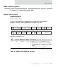
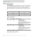
Bits Access Mnemonic Reset Description
Table 24: System Control register bit definition


