


www.digi.com
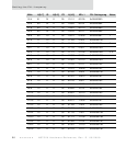
51
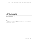
SYS Module
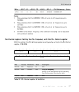
Note:
Using an external oscillator with PLL enabled is not advantageous, due to
the PLL input limitation of 10MHz to 20MHz. The oscillator needs to be the
same frequency as the crystal. Using a clock source greater than 20MHz
would result in the PLL running outside its operating range.
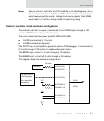
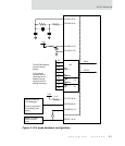
External oscillator mode hardware configuration
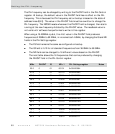
The external oscillator’s output is connected to the XTALA1 input through a 100
resistor. XTALA2 is an output and is left open.
The clock module has two power pins: PLLVDD and PLLVSS.
PLLVDD is connected to 1.5 volts
PLLVSS is connected to ground
The PLLTST input is connected to ground to use the JTAG debugger. It is connected to
3.3 volts through a 10K resistor to use boundary scan testing.
The BISTEN input is tied to 3.3 volts through a 10K resistor.
The SCANEN input is tied to 3.3 volts through a 10K resistor.
This diagram shows the hardware configuration:
XTALA1 (K14)
XTALA2 (K12)
PLLTST(N15)
BISTEN (M15)
SCANEN (L13)
PLLVDD (L15)
PLLVSS (L12)
BCLK
FXTAL
Oscillator
3.3V
1.5V
Tie high to use the
JTAG debugger
Connect to ground
to use boundary
scan testing
100 ohm