


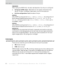

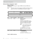

MEM module configuration
88
NS7520 Hardware Reference, Rev. D 03/2006
MEM module configuration
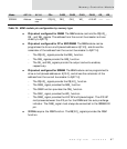
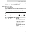
The MEM module is configured as shown in Table 35. Each chip select contains an
identical set of three registers that appear on a boundary of
’h10 bytes.
Each register is 32 bits unless otherwise noted.
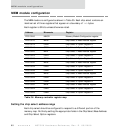
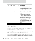
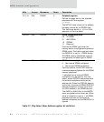
Setting the chip select address range
Each chip select should be configured to respond to a different portion of the
memory map. Do this by setting the appropriate fields in the Chip Select Base Address
and Chip Select Option registers.
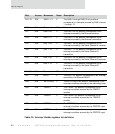
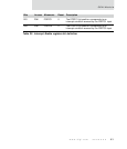
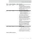
Address Mnemonic Register
FFC0 0000 MMCR Memory Module Configuration register
FFC0 0010 BAR0 Chip Select 0 Base Address register
FFC0 0014 OR0A Chip Select 0 Option Register A
FFC0 0018 OR0B Chip Select 0 Option Register B
FFC0 0020 BAR1 Chip Select 1 Base Address register
FFC0 0024 OR1A Chip Select 1 Option Register A
FFC0 0028 OR1B Chip Select 1 Option Register B
FFC0 0030 BAR2 Chip Select 2 Base Address register
FFC0 0034 OR2A Chip Select 2 Option Register A
FFC0 0038 OR2B Chip Select 2 Option Register B
FFC0 0040 BAR3 Chip Select 3 Base Address register
FFC0 0044 OR3A Chip Select 3 Option Register A
FFC0 0048 OR3B Chip Select 3 Option Register B
FFC0 0050 BAR4 Chip Select 4 Base Address register
FFC0 0054 OR4A Chip Select 4 Option Register A
FFC0 0058 OR4B Chip Select 4 Option Register B
Table 35: Memory controller register map