


www.digi.com
93
Memory Controller Module
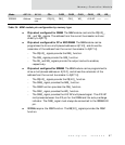
from address instead of chip select. The NS7520 provides the address signals during
the earliest part of each memory cycle. The CS0OE_ and CS0WE_ signals are
connected to the OE_ and WE_ input for the CS0 peripheral.
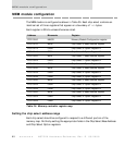
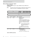
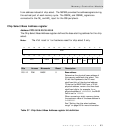
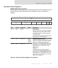
Chip Select Base Address register
Address: FFC0 0010/20/30/40/50
The Chip Select Base Address register defines the base starting address for the chip
select.
Note:
The V bit is set to 1 on hardware reset for chip select 0 only.
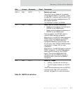
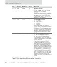
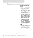
Bits Access Mnemonic Reset Description
D31:12 R/W BASE 0 Base address
Determines the physical base address of
the memory peripheral chip select. This
20-bit field represents the 20 most
significant bits of the physical address.
To derive the BASE field from a 32-bit
physical address, remove the three least
significant digits; for example, for a
physical address of
’h00200000, the BASE
field is set to ’h00200.
When accessing a static memory device,
the maximum value of the base address is
0x03000000.
See "Setting the chip select address
range" on page 88 for more information.
Table 37: Chip Select Base Address register bit definition
13121110987654321015 14
31 29 28 27 26 25 24 23 22 21 20 19 18 17 1630
BASE
BASE PGSIZE DMODE
DMUX
S
EXTTA
DMUX
M
IDLE
DR
SEL
BURST WP V