


www.digi.com
221
Serial Controller Module
exceeds a programmable interval. (See "Serial Channel 1, 2 Receive Character
Gap Timer," beginning on page 256, for more information.)
5 Configure Serial Channel Control Register B, as shown:
– RBGT: 1 to enable the buffer GAP timer
– RCGT: 1 to enable the character GAP timer
– MODE: 11 for slave mode
– BITORDR: user-defined
6 Configure Serial Channel Control Register A, as shown:
– CE: 1 for enable
– WLS: 11 for 8-bit operation
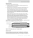
SPI slave transmitter
The SPI slave transmitter operates as follows:
Has the first bit ready for transmission before the SPI enable signal is
activated by the SPI master.
Changes the TXD output to the next data bit for transmission on the rising
edge of the SPI clock, while the SPI enable signal is active low.
Goes through a sampling of the SPI clock input. The output changes 3 to 4
internal system clock ticks from the rising edge of the SPI clock input. The
SPI master receiver does not sample the changing data until the next rising
edge of SPI clock.
Continues to change TXD data bits on the rising edge of SPI clock until the
SPI enable signal is driven inactive high. While the SPI enable signal is
inactive high, the TXD output remains constant.
SPI slave receiver
The SPI slave receiver operates as follows:
Samples the RXD input on the rising edge of the SPI clock signal while the
SPI enable signal is driven active low. The SPI slave receiver actually goes
through a sampling of the SPI input, which means the input is sampled 3 to 4
internal system clock ticks from the rising edge of the SPI clock input.
When the SPI slave receiver collects four bytes, these four bytes are written
to the RX FIFO. Receive data is read by the CPU or DMA controller from the
other side of the FIFO. If the SPI master transmitter always sends data in