


www.digi.com
45
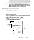
BBus Module
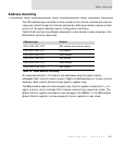
Address decoding
The CPU address map is divided to allow access to the internal modules and external
resources routed through the internal peripherals. Each slave module is given a small
portion of the system address map for configuration and status.
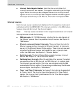
Table 20 defines how the address is decoded to allow access to slave modules or the
BUS module (external resources).
All resources defined in this manner are addressed using the upper memory
addresses. Each internal module is given 1 Mbyte of address space for its own internal
decoding. Each module defines its own specific register map.
The BBus module does not allow access to any internal registers unless the
CPU_SUPV
signal is active, which indicates that firmware is executing in supervisor mode. The
System Control register provides an override signal (the USER bit in the GEN module
System Control register) to allow access to internal registers in user mode.
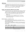
Address range Module
0000 0000–FF6F FFFF BUS module and external memory
FF80 0000–FF8F FFFF EFE module
FF90 0000–FF9F FFFF DMA module
FFB0 0000–FFBF FFFF GEN module
FFC0 0000–FFCF FFFF MEM module
FFD0 0000–FFDF FFFF SER module
Table 20: BBus address decoding