


MEMORY CONTROLLER S3C2410A
5-14
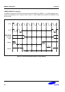
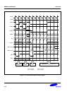
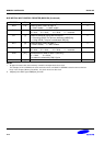
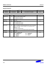
BUS WIDTH & WAIT CONTROL REGISTER (BWSCON) (Continued)
BWSCON Bit Description Initial state
WS2 [10] Determine WAIT status for bank 2.
0 = WAIT disable 1 = WAIT enable
0
DW2 [9:8] Determine data bus width for bank 2.
00 = 8-bit 01 = 16-bit, 10 = 32-bit 11 = reserved
0
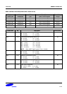
ST1 [7] Determine SRAM for using UB/LB for bank 1.
0 = Not using UB/LB (The pins are dedicated nWBE[3:0])
1 = Using UB/LB (The pins are dedicated nBE[3:0])
0
WS1 [6] Determine WAIT status for bank 1.
0 = WAIT disable, 1 = WAIT enable
0
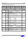
DW1 [5:4] Determine data bus width for bank 1.
00 = 8-bit 01 = 16-bit, 10 = 32-bit 11 = reserved
0
DW0 [2:1] Indicate data bus width for bank 0 (read only).
01 = 16-bit, 10 = 32-bit
The states are selected by OM[1:0] pins
-
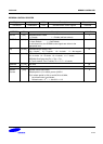
Reserved [0] -
NOTES:
1. All types of master clock in this memory controller correspond to the bus clock.
For example, HCLK in SRAM is the same as the bus clock, and SCLK in SDRAM is also the same as the bus
clock. In this chapter (Memory Controller), one clock means one bus clock.
2. nBE[3:0] is the 'AND' signal nWBE[3:0] and nOE.