


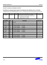

LCD CONTROLLER S3C2410A
15-4
STN LCD CONTROLLER OPERATION
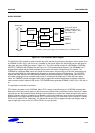
TIMING GENERATOR (TIMEGEN)
The TIMEGEN generates the control signals for the LCD driver, such as VFRAME, VLINE, VCLK, and VM. These
control signals are closely related to the configuration on the LCDCON1/2/3/4/5 registers in the REGBANK. Based
on these programmable configurations on the LCD control registers in the REGBANK, the TIMEGEN can generate
the programmable control signals suitable to support many different types of LCD drivers.
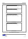
The VFRAME pulse is asserted for the duration of the entire first line at a frequency of once per frame. The VFRAME
signal is asserted to bring the LCD's line pointer to the top of the display to start over.
The VM signal helps the LCD driver alternate the polarity of the row and column voltages, which are used to turn the
pixel on and off. The toggling rate of VM signals depends on the MMODE bit of the LCDCON1 register and MVAL
field of the LCDCON4 register. If the MMODE bit is 0, the VM signal is configured to toggle on every frame. If the
MMODE bit is 1, the VM signal is configured to toggle on the every event of the elapse of the specified number of
VLINE by the MVAL[7:0] value. Figure 15-4 shows an example for MMODE = 0 and for MMODE = 1 with the value of
MVAL[7:0] = 0x2. When MMODE = 1, the VM rate is related to MVAL[7:0], as shown below:
VM Rate = VLINE Rate / ( 2 * MVAL)
The VFRAME and VLINE pulse generation relies on the configurations of the HOZVAL field and the LINEVAL field in
the LCDCON2/3 register. Each field is related to the LCD size and display mode. In other words, the HOZVAL and
LINEVAL can be determined by the size of the LCD panel and the display mode according to the following equation:
HOZVAL = (Horizontal display size / Number of the valid VD data line)-1
In color mode: Horizontal display size = 3 * Number of Horizontal Pixel
In the 4-bit single scan display mode, the Number of valid VD data line should be 4. In case of 4-bit dual scan
display, the Number of valid VD data line should also be 4 while in case of 8-bit single scan display mode, the
Number of valid VD data line should be 8.
LINEVAL = (Vertical display size) -1: In case of single scan display type
LINEVAL = (Vertical display size / 2) -1: In case of dual scan display type
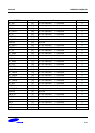
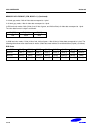
The rate of VCLK signal depends on the configuration of the CLKVAL field in the LCDCON1 register. Table 15-1
defines the relationship of VCLK and CLKVAL. The minimum value of CLKVAL is 2.
VCLK(Hz)=HCLK/(CLKVAL x 2)
The frame rate is the VFRAM signal frequency. The frame rate is closely related to the field of WLH[1:0](VLINE pulse
width) WDLY[1:0] (the delay width of VCLK after VLINE pulse), HOZVAL, LINEBLANK, and LINEVAL in the
LCDCON1/2/3/4 registers as well as VCLK and HCLK. Most LCD drivers need their own adequate frame rate. The
frame rate is calculated as follows:
frame_rate(Hz) = 1 / [ { (1/VCLK) × (HOZVAL+1)+(1/HCLK) × (A+B+(LINEBLANK × 8) ) } × ( LINEVAL+1) ]
A = 2
(4+WLH)
, B = 2
(4+WDLY)