


ARM920T PROCESSOR MMU
3-9
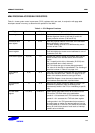
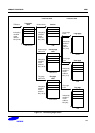
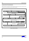
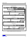
SECTION DESCRIPTOR
Bits 3:2 (C & B) indicate whether the area of memory mapped by this section is treated as write-back cacheable,
write-through cacheable, non-cached buffered or non-cached non-buffered.
Bit 4 should be written to 1 for backward compatibility.
Bits 8:5 specify one of the 16 possible domains (held in the domain access control registers) that contain the
primary access controls.
Bit 9 is always written as 0.
Bits 11:10 (AP) specify the access permissions for this section.
Bits 19:12 are always written as 0.
Bits 31:20 form the corresponding bits of the physical address for a section.
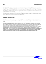
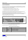
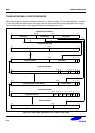
COARSE PAGE TABLE DESCRIPTOR
Bits 3:2 are always written as 0.
Bit 4 is always written as 1.
Bits 8:5 specify one of the 16 possible domains (held in the Domain access control registers) that contain the
primary access controls.
Bit 9 is always written as 0.
Bits 31:10 form the base for referencing the level two descriptor. (The coarse page table index for the entry is derived
from the modified virtual address.)
If a coarse page table descriptor is returned from the level one fetch, a level two fetch is initiated.
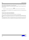
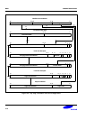
FINE PAGE TABLE DESCRIPTOR
Bits 3:2 are always written as 0.
Bit 4 is always written as 1.
Bits 8:5 specify one of the 16 possible domains (held in the domain access control registers) that contain the
primary access controls.
Bits 11:9 are always written as 0.
Bits 31:12 form the base for referencing the level two descriptor. (The fine page table index for the entry is derived
from the modified virtual address.)
If a fine page table descriptor is returned from the level one fetch, a level two fetch is initiated.