


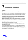
CLOCK & POWER MANAGEMENT S3C2410A
7-2
FUNCTIONAL DESCRIPTION
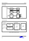
CLOCK ARCHITECTURE
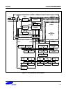
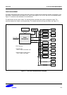
Figure 7-1 shows a block diagram of the clock architecture. The main clock source comes from an external crystal
(XTIpll) or an external clock (EXTCLK). The clock generator includes an oscillator (Oscillation Amplifier), which is
connected to an external crystal, and also has two PLLs (Phase-Locked-Loop), which generate the high frequency
clock required in the S3C2410A.
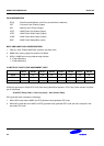
CLOCK SOURCE SELECTION
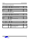
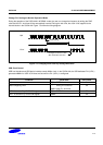
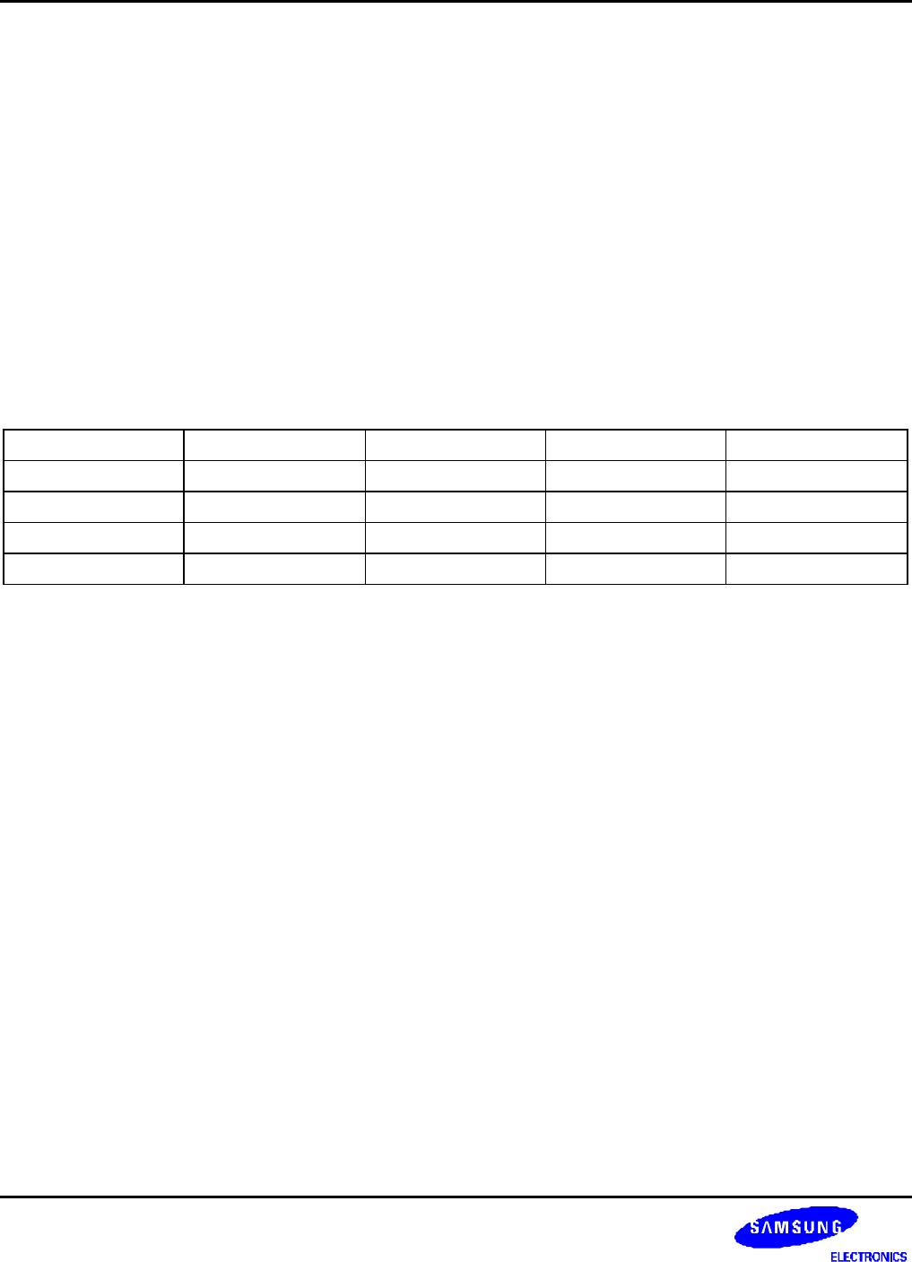
Table 7-1 shows the relationship between the combination of mode control pins (OM3 and OM2) and the selection of
source clock for the S3C2410A. The OM[3:2] status is latched internally by referring the OM3 and OM2 pins at the
rising edge of nRESET.
Table 7-1. Clock Source Selection at Boot-Up
Mode OM[3:2] MPLL State UPLL State Main Clock source USB Clock Source
00 On On Crystal Crystal
01 On On Crystal EXTCLK
10 On On EXTCLK Crystal
11 On On EXTCLK EXTCLK
NOTES:
1. Although the MPLL starts just after a reset, the MPLL output (Mpll) is not used as the system clock until the software
writes valid settings to the MPLLCON register. Before this valid setting, the clock from external crystal or EXTCLK source
will be used as the system clock directly. Even if the user does not want to change the default value of MPLLCON
register, the user should write the same value into MPLLCON register.
2. OM[3:2] is used to determine a test mode when OM[1:0] is 11.