PRODUCT OVERVIEW S3C2410A
1-18
Table 1-2. 272-Pin FBGA Pin Assignments (Continued)
Pin
Number
Pin
Name
Default
Function
I/O State
@BUS REQ
I/O State
@PWR-off
I/O State
@nRESET
I/O Type
E6 VSSMOP VSSMOP P P P s3o
C4 VDDi VDDi P P P d1c
F6 VSSi VSSi P P P s3i
A3 DATA16 DATA16 Hi-z Hi-z Hi-z t12
B3 DATA17 DATA17 Hi-z Hi-z Hi-z t12
A2 DATA18 DATA18 Hi-z Hi-z Hi-z t12
A1 DATA19 DATA19 Hi-z Hi-z Hi-z t12
B2 DATA20 DATA20 Hi-z Hi-z Hi-z t12
NOTES:
1. The @BUS REQ. shows the pin states at the external bus, which is used by the other bus master.
2. ' – ‘ mark indicates the unchanged pin state at Bus Request mode.
3. Hi-z or Pre means Hi-z or Previous state and it is determined by the setting of MISCCR register.
4. AI/AO means analog input/analog output.
5. P, I, and O mean power, input and output respectively.
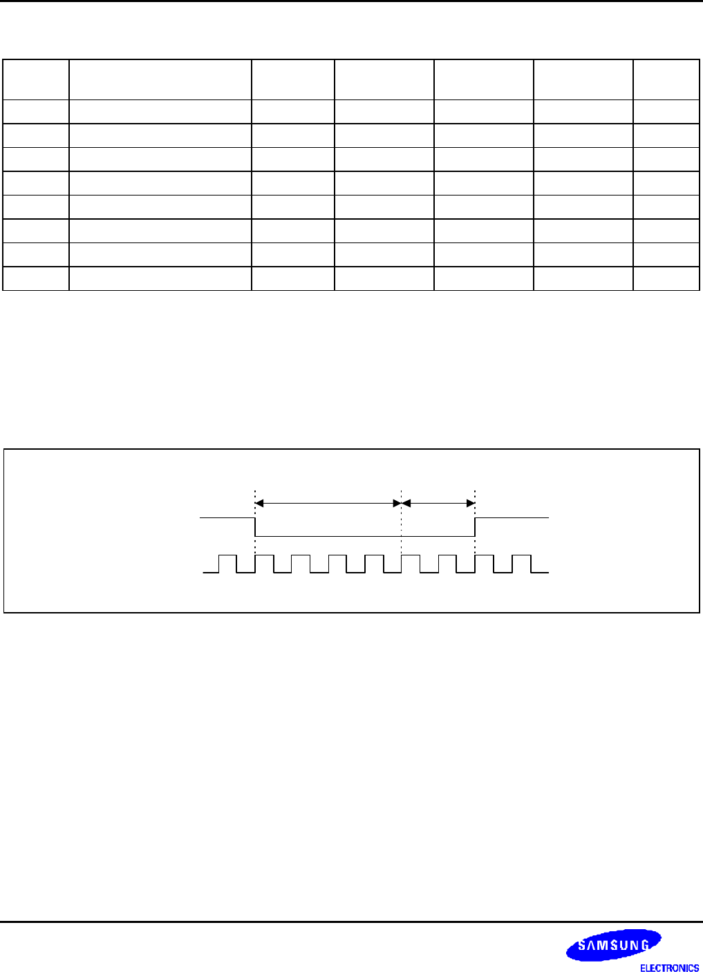
6. The I/O state @nRESET shows the pin status in the @nRESET duration below.
nRESET
FCLK
@nRESET4FCLK


