


CACHES, WRITE BUFFER ARM920T PROCESSOR
4-6
DATA CACHE AND WRITE BUFFER ENABLE/DISABLE
On reset, all DCache entries are invalidated, the DCache is disabled, and the write buffer contents are discarded.
There is no explicit write buffer enable bit implemented in ARM920T. Situations in which the write buffer is used are
described below.
The DCache is enabled by writing 1 to the Ccr bit, and disabled by writing 0 to the Ccr bit.
The DCache must be enabled only when the MMU is enabled. This is because the MMU translation tables define the
cache and write buffer configuration for each memory region.
When the DCache is disabled the cache contents are ignored and all data accesses appear on the Advanced
System Bus as separate non-sequential accesses. If the cache is subsequently re-enabled its contents will be
unchanged. Depending on the software system design, the cache may need to be cleaned after it is disabled, and
invalidated before it is re-enabled. See Cache coherence on page 4-10.
The MMU and DCache can be enabled or disabled simultaneously with a single MCR which changes bit 0 and bit 2
in the control register (CP15 register 1).
DATA CACHE AND WRITE BUFFER OPERATION
The DCache and write buffer configuration of each memory region is controlled by the C and B bits in each section
and page descriptor in the MMU translation tables. For clarity, these bits are referred to as Ctt and Btt in the
following text. The configuration is modified by the DCache enable bit in the CP15 control register, which is referred
to as Ccr.
If the DCache is enabled, a DCache lookup is performed for each data access initiated by the ARM9TDMI CPU core,
regardless of the value of the Ctt bit in the relevant MMU translation table descriptor. If the accessed virtual address
matches the virtual address of an entry in the cache, the lookup is called a cache hit. If the required address does
not match any entry in the cache, the lookup is called a cache miss. In this context a data access means any type
of load (read) or store (write) or swap instruction, including LDR, LDRB, LDRH, LDM, LDC, STR, STRB, STRH, STC,
SWP and SWPB.
To ensure that accesses appear on the ASB in program order, ARM920T will wait for all writes in the write buffer to
complete on the ASB before starting any other ASB access. The ARM9TDMI CPU core can continue executing at
full speed reading instructions and data from the caches and writing to the DCache and write buffer while buffered
writes are being written to memory via the ASB.
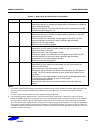
Table 4-1 describes the DCache and write buffer behavior for each type of memory configuration. Ctt AND Ccr means
the bitwise Boolean AND of Ctt with Ccr.